

Memory element and memory device
A storage element and storage layer technology, applied in electrical components, information storage, static memory, etc., can solve problems such as difficult current flow, thin address wiring, etc., to eliminate operating errors, reduce write current, and improve magnetic properties. anisotropic effect
Active Publication Date: 2012-04-04
SONY CORP
View PDF8 Cites 0 Cited by
- Summary
- Abstract
- Description
- Claims
- Application Information
AI Technical Summary
Problems solved by technology
[0015] However, as the size of the elements that make up the MRAM is reduced, the address wiring becomes thinner, making it difficult to pass a sufficient current
Method used
View moreImage
Smart ImageViewing Examples

Examples
Embodiment approach
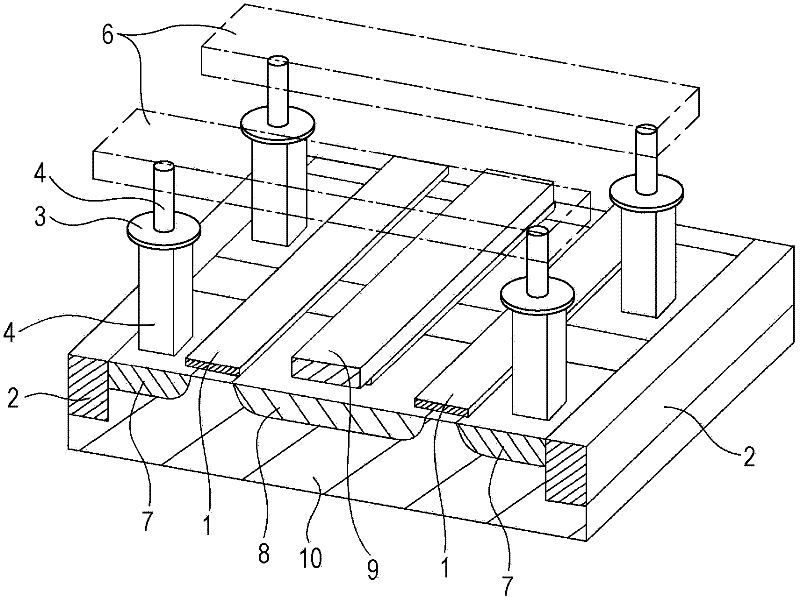
[0068] 1. Outline of the memory element of the embodiment
[0069] 2. Structure of Embodiment
Login to View More PUM
| Property | Measurement | Unit |
|---|---|---|
| Thickness | aaaaa | aaaaa |
| Current density | aaaaa | aaaaa |
| Film thickness | aaaaa | aaaaa |
Abstract
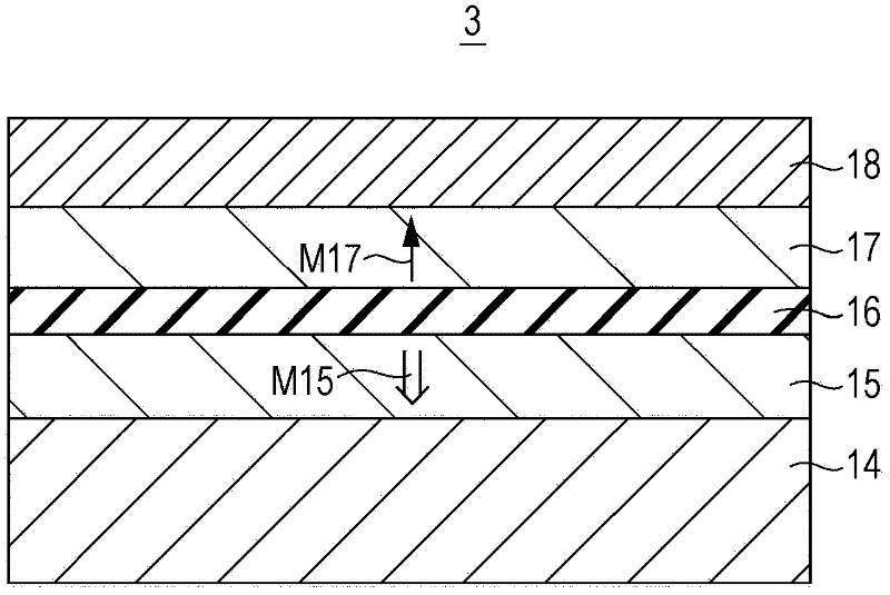
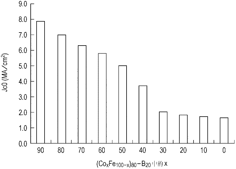
The present invention discloses a memory element and a memory device. The memory element a memory layer that has a magnetization perpendicular to a film face and a magnetization direction thereof varies corresponding to information; a magnetization-fixed layer that has a magnetization that is perpendicular to the film face; and an insulating layer that is provided between the memory layer and the magnetization-fixed layer, wherein the memory layer has a lamination structure of a Co-Fe-B layer and an element belonging to any one of 1A group, 2A group, 3A group, 5A group, or 6A group, an electron that is spin-polarized is injected in a lamination direction of a layered structure, and thereby the magnetization direction of the memory layer varies and a recording of information is performed with respect to the memory layer, a magnitude of an effective diamagnetic field which the memory layer receives is smaller than a saturated magnetization amount of the memory layer.
Description
technical field [0001] The present invention relates to a memory element including a memory layer storing the magnetization state of a ferromagnetic layer as information and a magnetization fixed layer whose magnetization direction is fixed, and changing the magnetization direction of the memory layer by passing an electric current. The invention also relates to a storage device with the storage element. Background technique [0002] In information devices such as computers, high-density DRAMs operating at high speeds have been widely used as random access memories. [0003] However, DRAM is a volatile memory in which information is erased when power is turned off, and therefore, a nonvolatile memory in which information is not erased is desired. [0004] In addition, Magnetic Random Access Memory (MRAM), which records information by magnetization of a magnetic material, has attracted attention as an alternative nonvolatile memory, and thus has been developed. [0005] MRA...
Claims
Login to View More Application Information
Patent Timeline
 IPC IPC(8): G11C11/16H01L43/08
CPCG11C11/16H01L43/08H01L43/10H01L27/228G11C11/161G11C11/1675H10B61/22H10N50/85H10N50/10G11C7/04
Inventor细见政功别所和宏大森广之肥后丰山根一阳内田裕行
OwnerSONY CORP