
Quick fuse for protection of semiconductor devices

A semiconductor and fuse link technology, applied in emergency protection devices, electrical components, circuits, etc., can solve the problems of complex manufacturing process, large space occupation, unfavorable heat dissipation, etc. Effect

Inactive Publication Date: 2012-04-04
上海电器陶瓷厂有限公司
View PDF3 Cites 4 Cited by
  • Summary
  • Abstract
  • Description
  • Claims
  • Application Information

AI Technical Summary

Problems solved by technology

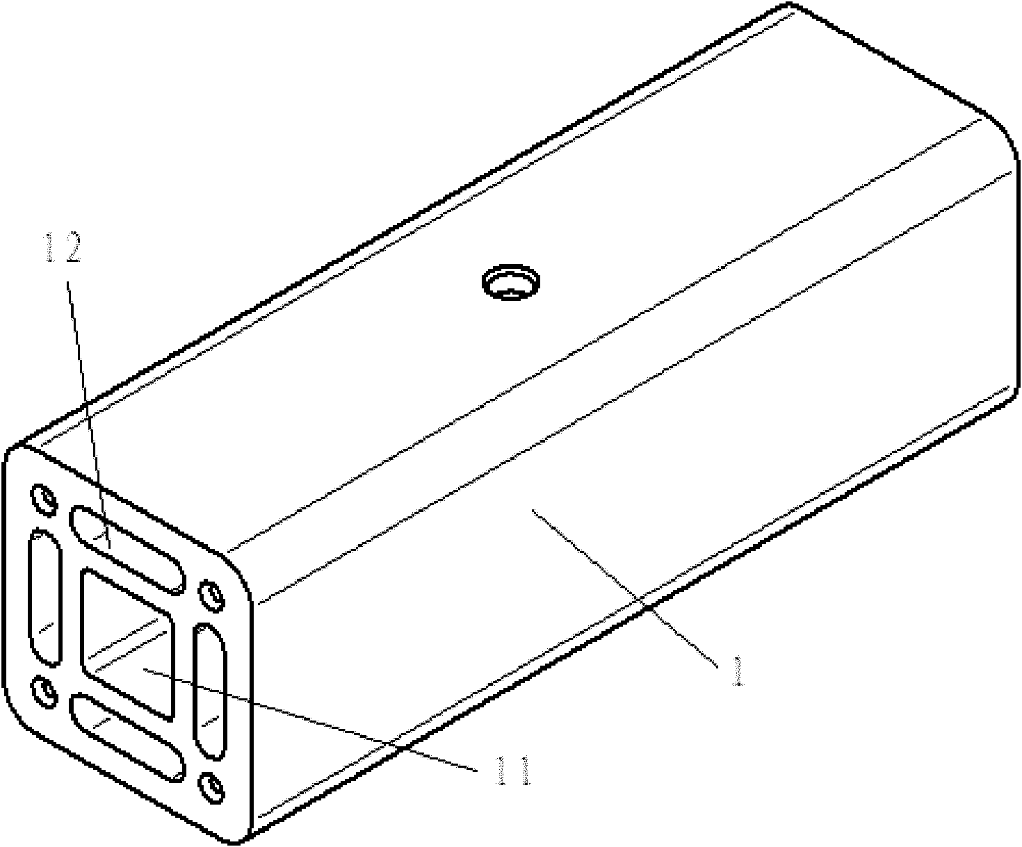
Since the heat dissipation cavity 11 and the melt cavity 12 are isolated, the manufacturing process of the melting tube is relatively complicated and is not conducive to good heat dissipation
In addition, its monomer capacity can reach up to 1800V DC, 250A, but if you want to use it in the occasion of 1800V DC, 500A, you need to use two monomers with a capacity of 1800V DC and 250A DC fuses in parallel. For other capacity levels, multiple monomers with lower voltage and higher current are used in series or in parallel, which not only takes up a lot of space, but also wastes resources.

Method used


Image

  • Quick fuse for protection of semiconductor devices
  • Quick fuse for protection of semiconductor devices
  • Quick fuse for protection of semiconductor devices

Examples


Embodiment Construction

[0030] In order to better understand the technical solution of the present invention, it will be described in detail below through specific embodiments in conjunction with the accompanying drawings:

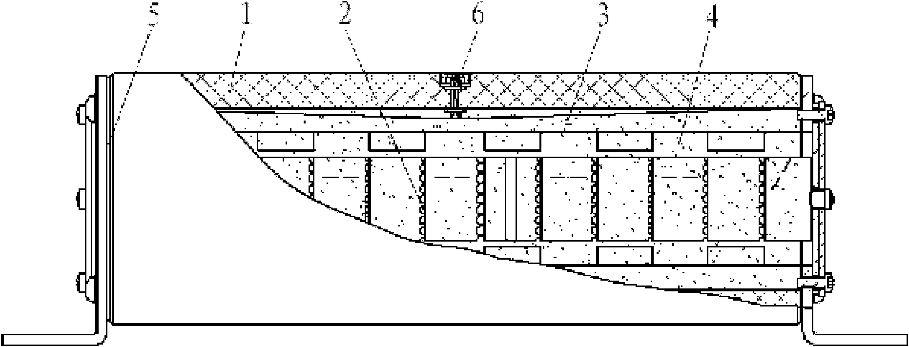
[0031] see Figure 2 to Figure 7 , the semiconductor device protection fast fuse of the present invention includes a melting tube 1, four melts 2, an arc extinguishing medium 4, a pair of contact plates 5 and an indicator 6, wherein:

[0032] The outer surface of the melting tube 1 is a regular square prism, which is made of No. 95 alumina ceramic insulating material, which has good high temperature resistance and mechanical properties, and is also more beautiful in appearance; the center of the end face of the melting tube 1 has a cavity with a regular quadrilateral cross section. 10. The cavity 10 is used not only as an installation cavity for the melt 2, but also as a cooling cavity; a radial perforation connecting the cavity 10 is provided on the wall of the melting tube 1; ...


PUM


Abstract

The invention discloses a quick fuse for protection of semiconductor devices, which comprises a fusion tube, a plurality of fusion sheets, arc extinguishing media and a pair of contact plates. A cavity is axially arranged on the central end face of the fusion tube, a solder bridge is arranged on the surface of each fusion sheet, multicolumn large holes are uniformly arranged at intervals on the surface of the each fusion sheet, small holes in column are arranged beside each column of large holes, each column of large holes comprises a plurality of large-diameter holes with same sizes, and each column of small holes comprises a plurality of small-diameter holes with same sizes. The large holes in column close to the length center of the corresponding fusion sheet are transverse elongated holes, and another column of small holes is further arranged between the column of elongated holes and the column of small holes close to the elongated holes. Each fusion sheet is bent into a square wave shape with center lines of the large holes in column and the small holes in column serving as folding lines, and then inserted into the cavity of the fusion tube after being enclosed into a shape with an open equilateral polygonal section. The arc extinguishing media are filled between a cavity of each fusion sheet and the corresponding fusion sheet, and the contact plates in pair are fastened to two ends of the fusion tube.

Description

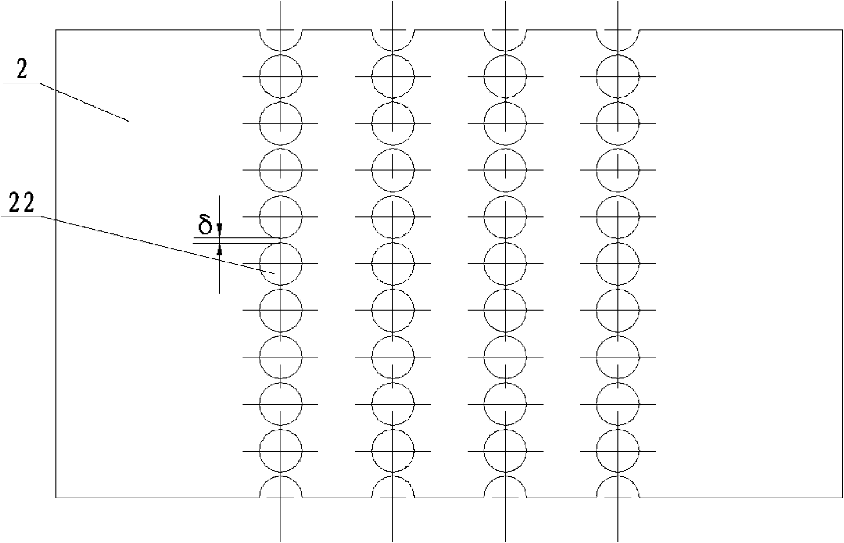
technical field [0001] The invention relates to a fast fuse for semiconductor equipment protection, which is suitable for a rated DC voltage of 1800V DC and a rated current of 250A to 500A. Background technique [0002] Fuse links for semiconductor equipment protection (hereinafter referred to as fuse links) are used for short-circuit protection of rectifier equipment and related equipment (including frequency converters, soft starters, etc.), semiconductor components and complete sets of equipment composed of them, and are suitable for DC circuits. The fuse includes a fusion tube, a melt in the fusion tube and contact plates at both ends of the fusion tube. Each melt 2 is welded with tin bridges and has several rows of small holes 22 of equal diameter (see FIG. 1 ). When a large short-circuit current passes through the melt, the narrow neck δ between the small holes is rapidly heated due to the thermal effect of the current, and the local temperature rises rapidly until the...

Claims


Application Information

Patent Timeline
IPC IPC(8): H01H85/042H01H85/05H01H85/11H01H85/38
Inventor 林海鸥戎峰陈妍吴辉徐鹤
Owner 上海电器陶瓷厂有限公司
Learn More