Fabricating method for photoelectric element base

A technology of photoelectric components and manufacturing methods, which is applied in the direction of electrical components, circuits, semiconductor devices, etc., can solve the problems of inconvenience, time-consuming, and additional welding of grounding pins, and achieve the effects of reducing costs, improving product quality, and shortening molding time

Inactive Publication Date: 2014-12-17
CORETEK OPTO CORP
View PDF4 Cites 0 Cited by
  • Summary
  • Abstract
  • Description
  • Claims
  • Application Information

AI Technical Summary

Problems solved by technology

[0013] The purpose of the present invention is to provide a base manufacturing method for photoelectric components, which mainly adopts a continuous combination type, which improves the inconvenience and time-consuming lack of conventional bases that need to be fabricated one by one, and the lack of additional welding for grounding pins

Method used


Image

  • Fabricating method for photoelectric element base
  • Fabricating method for photoelectric element base
  • Fabricating method for photoelectric element base

Examples


Embodiment Construction

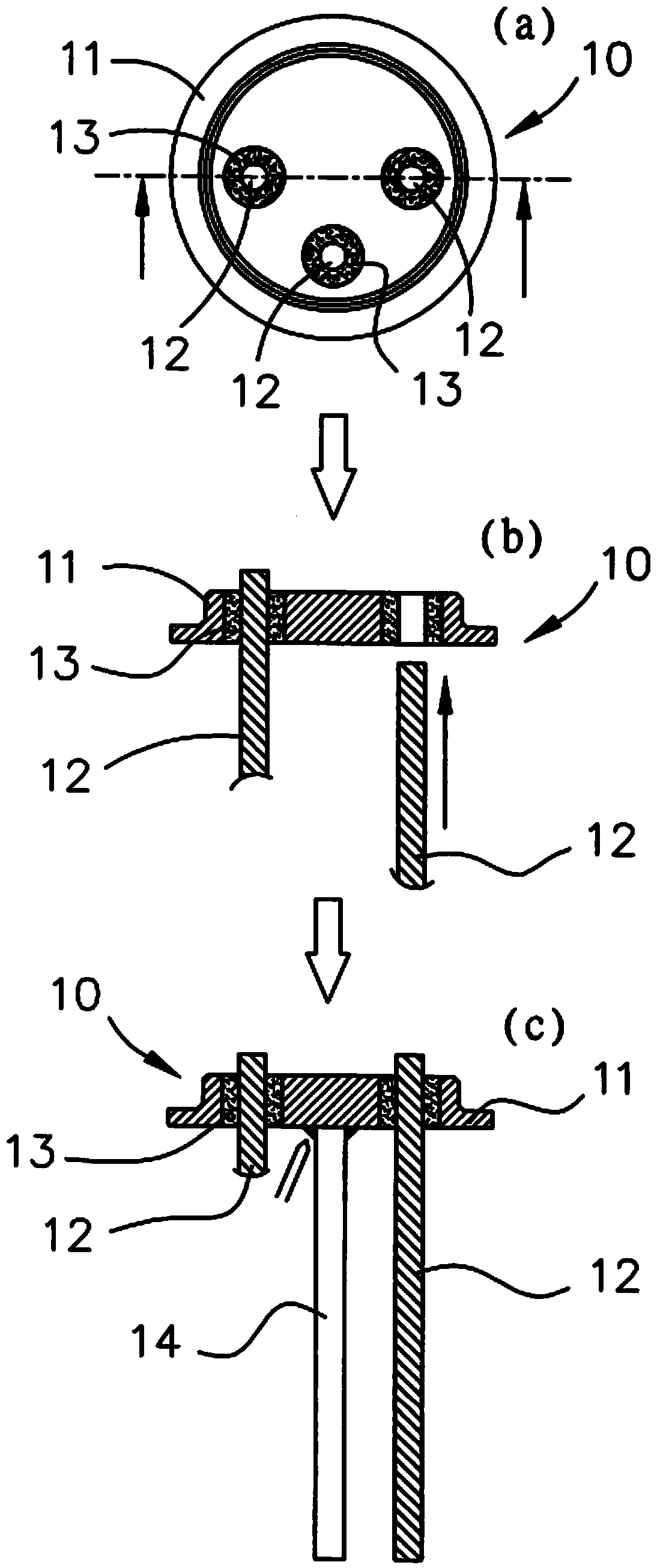
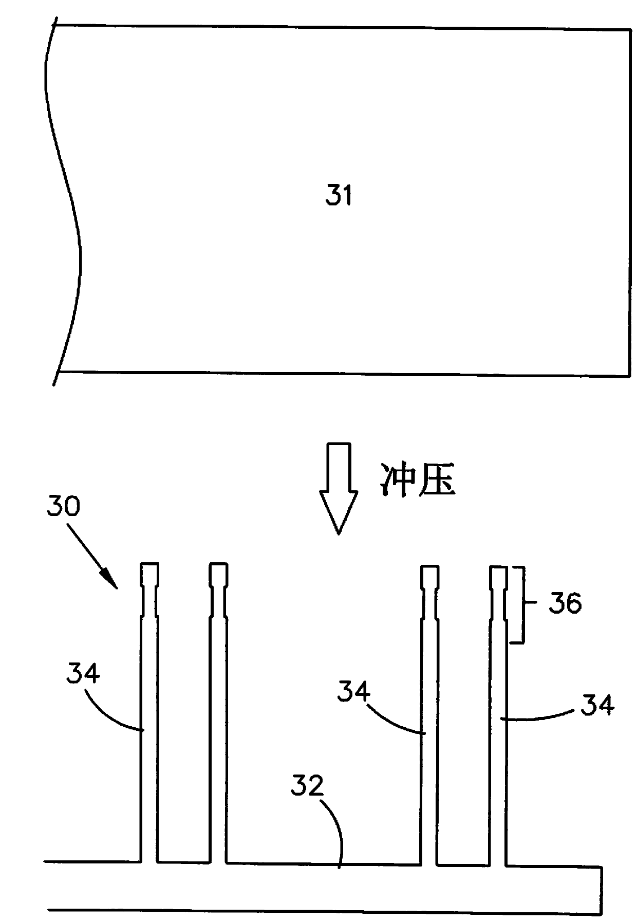
[0107] see image 3 , the figure shows the method of making a support substrate 30, which is to take a metal material (continuous metal strip or sheet metal plate) 31, and form a strip 32 with multiple pins 34 by stamping . Above-mentioned pin 34 can define an electroplating area 36 from free end; This electroplating area 36 is less than 1 / 2nd of the length of pin 34; For example, if the length of pin 34 is 15mm, then electroplating area 36 is no more than 7.5 mm; generally speaking, according to the length of different types of pins 34 and the convenience of electroplating processing, the length of the electroplating area 36 is mostly between 1 mm and 5 mm.

[0108] Figure 4 The display bracket substrate 30 can face an electroplating tank 38 and allow the electroplating area 36 of each pin 34 to enter the electroplating solution. In this way, a layer of metal is attached to the surface of the electroplating area 36; the metal attached to the electroplating area 36 is pref...


PUM


Abstract

The invention relates to a fabricating method for a photoelectric element base, which comprises the steps of fabricating a support substrate, plating pins limitedly, assembling the pins and a metallic disc, injecting plastic materials in mould closing and cutting tapes. According to implementation of the steps, the support substrate with a plurality of limitedly plating pins and the metallic disc can be combined continuously by injecting the plastic materials and then properly cut so that an independent element can be acquired. The fabricating method for the photoelectric element base has the advantages of simplicity, convenience and time saving in fabrication, low cost, high yield and the like.

Description

technical field [0001] The invention relates to a photoelectric element, especially a method for making a base of the photoelectric element. Background technique [0002] A general photoelectric element is formed by disposing a photoelectric chip on a base; the base can be a combination of a metal plate, a plurality of conductive pins and a ground guide. [0003] see figure 1 , the figure shows that the base 10 of a photoelectric element is to take a metal disc body 11, and a plurality of independent pins 12 are respectively inserted on the metal disc body 11; then fill between the pins 12 and the metal disc body 11 glass material 13, and the glass material 13, the pin 12 and the metal plate 11 are combined together by glass sintering. Another ground pin 14 can be combined with the metal plate 11 by spot welding or laser welding. This results in a single and independent base. [0004] Then put each base 10 into a barrel plating bath for full plating treatment (not shown)...

Claims


Application Information

Patent Timeline
Patent Type & Authority Patents(China)
IPC IPC(8): H01L31/18
CPCY02P70/50
Inventor 袁荣亨田荣蒋
Owner CORETEK OPTO CORP
Why Eureka
Try Eureka