Testing structure capable of effectively testing shallow trench isolation filling capability

A technology for testing structure and filling capability, applied in semiconductor/solid-state device testing/measurement, electrical components, electrical solid-state devices, etc., can solve problems such as inability to obtain STI filling capability, generation of holes 202, and inconsistent depth of etching test structures

Inactive Publication Date: 2012-04-11
SHANGHAI HUALI MICROELECTRONICS CORP
View PDF5 Cites 0 Cited by
  • Summary
  • Abstract
  • Description
  • Claims
  • Application Information

AI Technical Summary

Problems solved by technology

[0007] However, due to the loading effect of the STI etching process, such a situation may result: the two outer trenches 203 on both sides of the outermost periphery of the test structure are usually deeper than the first trench 200 in the middle, and the two outer trenches The groove 203 also fluctuates along with the change of the surrounding dummy structure 204, so that the hole 202 is easily generated during the STI filling process, wherein the hole 202 is located between the outermost two of the first silicon substrate lines 201, refer to figure 2 The outermost silicon base line 206 and the second outer silicon base line 205 in
[0008] It can be seen that the defect of the prior art is that the depth of the grooves on the outermost sides of the etching test structure is inconsistent during the STI etching process, so that the actual filling ability of the STI cannot be obtained.

Method used


Image

  • Testing structure capable of effectively testing shallow trench isolation filling capability
  • Testing structure capable of effectively testing shallow trench isolation filling capability
  • Testing structure capable of effectively testing shallow trench isolation filling capability

Examples


Embodiment Construction

[0022] An effective test structure for testing the filling capability of shallow trench isolation of the present invention will be described in further detail below with reference to the accompanying drawings and specific embodiments.

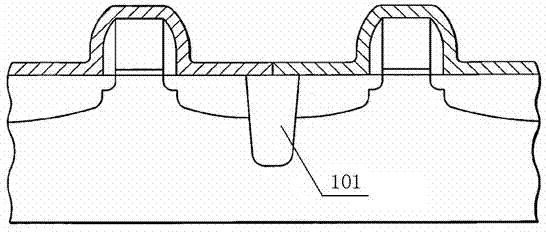
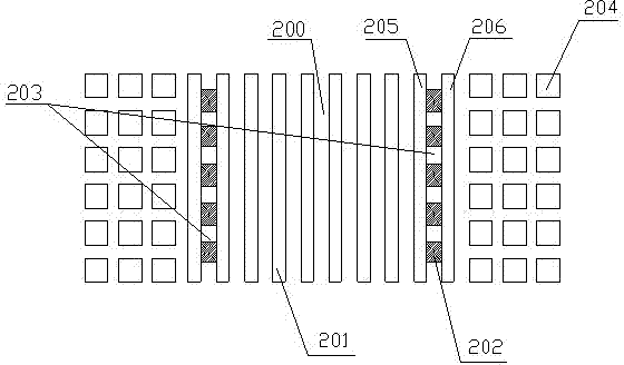
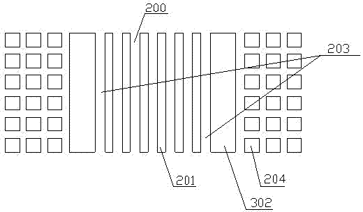
[0023] image 3 A schematic diagram of a test structure for effectively testing the filling capability of shallow trench isolation according to a preferred embodiment of the present invention is shown. Specifically, on silicon substrates ( image 3 Not marked in, you can refer to figure 2 A number of first trenches 200 for forming shallow trench test structures are etched on the silicon substrate 201 in The trenches 200 are distributed in the middle of the test structure, image 3 Among the outermost trenches 203, those skilled in the art understand that the outermost trenches 203 are also the first trenches 200, and the difference from other first trenches 200 is that the outermost trenches 203 are part of the test structure. The outermos...


PUM


Abstract

The invention discloses a testing structure capable of effectively testing shallow trench isolation filling capability. A plurality of first trenches for the formation of the shallow trench testing structure are etched on a silicon substrate, a first silicon substrate line is formed on the silicon substrate between each two neighboring first trenches, the first trenches are distributed at the middle of the testing structure, and a plurality of virtual structures which are used for eliminating the loading effect in the chemical mechanical polishing process are also arranged outside the testing structure. The testing structure is characterized in that: in the testing structure, second silicon substrate lines are formed at the outer sides of the outmost first trenches, and the width of the second silicon substrate line is greater than the width of the first silicon substrate line. The testing structure has the advantages that: by moderately increasing the width of the outmost silicon substrate lines on both sides in the STI (shallow trench isolation) filling capability testing structure, the loading effect caused by STI etching is eliminated, and thereby the testing structure can more effectively provide information for engineers to judge or debug the STI filling process.

Description

technical field [0001] The invention relates to the technical field of integrated circuit manufacturing, in particular to an effective test structure for testing the filling capability of shallow trench isolation. Background technique [0002] CMOS (Complementary Metal-Oxide-Semiconductor Transistor) process refers to a complementary MOS integrated circuit manufacturing process composed of complementary metal oxides (PMOS transistors and NMOS transistors), which is characterized by low power consumption. Since the gate circuit composed of a pair of MOS in CMOS is viewed in an instant, either the PMOS is turned on, or the NMOS is turned on, or both are turned off, which is much more efficient than a linear triode (BJT), so the power consumption is very low. [0003] At present, when the CMOS process develops below 0.25um, the reference figure 1 Shown is a cross-sectional view of device isolation currently widely used in processes below 0.25um. People gradually use Shallow T...

Claims


Application Information

Patent Timeline
Patent Type & Authority Applications(China)
IPC IPC(8): H01L23/544H01L21/66
Inventor 徐强张文广郑春生陈玉文
Owner SHANGHAI HUALI MICROELECTRONICS CORP
Why Eureka
Try Eureka