Pixel circuit and driving method thereof

A technology of a pixel circuit and a driving method, which is applied in the field of pixel circuits and their driving, can solve the problems of limited time for writing data, limited time for writing data, and the maximum frame rate of a panel, etc., and achieves the effect of improving the feasibility

Active Publication Date: 2012-05-02
AU OPTRONICS CORP
View PDF3 Cites 47 Cited by
  • Summary
  • Abstract
  • Description
  • Claims
  • Application Information

AI Technical Summary

Problems solved by technology

According to the existing compensation technology, it is necessary to reset the data and compensate the critical voltage (V TH ) and writing data and other three operations, once the frame rate is too high, the time that can be used to write data will be extre

Method used


Image

  • Pixel circuit and driving method thereof
  • Pixel circuit and driving method thereof
  • Pixel circuit and driving method thereof

Examples


Embodiment Construction

[0053] The brightness displayed by an organic light emitting diode (Organic Light Emitting Diode, OLED) is determined by the magnitude of the current flowing through it. For an active matrix OLED (AMOLED), the current flowing through the OLED is determined by a driven thin film transistor (Thin Film Transistor, TFT). Therefore, any factor related to TFT or OLED may affect the display quality of AMOLED.

[0054] Therefore, the present invention provides a pixel circuit and its driving method to solve the above-mentioned shortcomings.

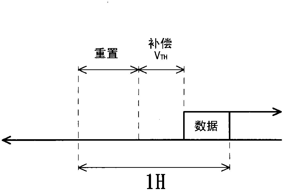
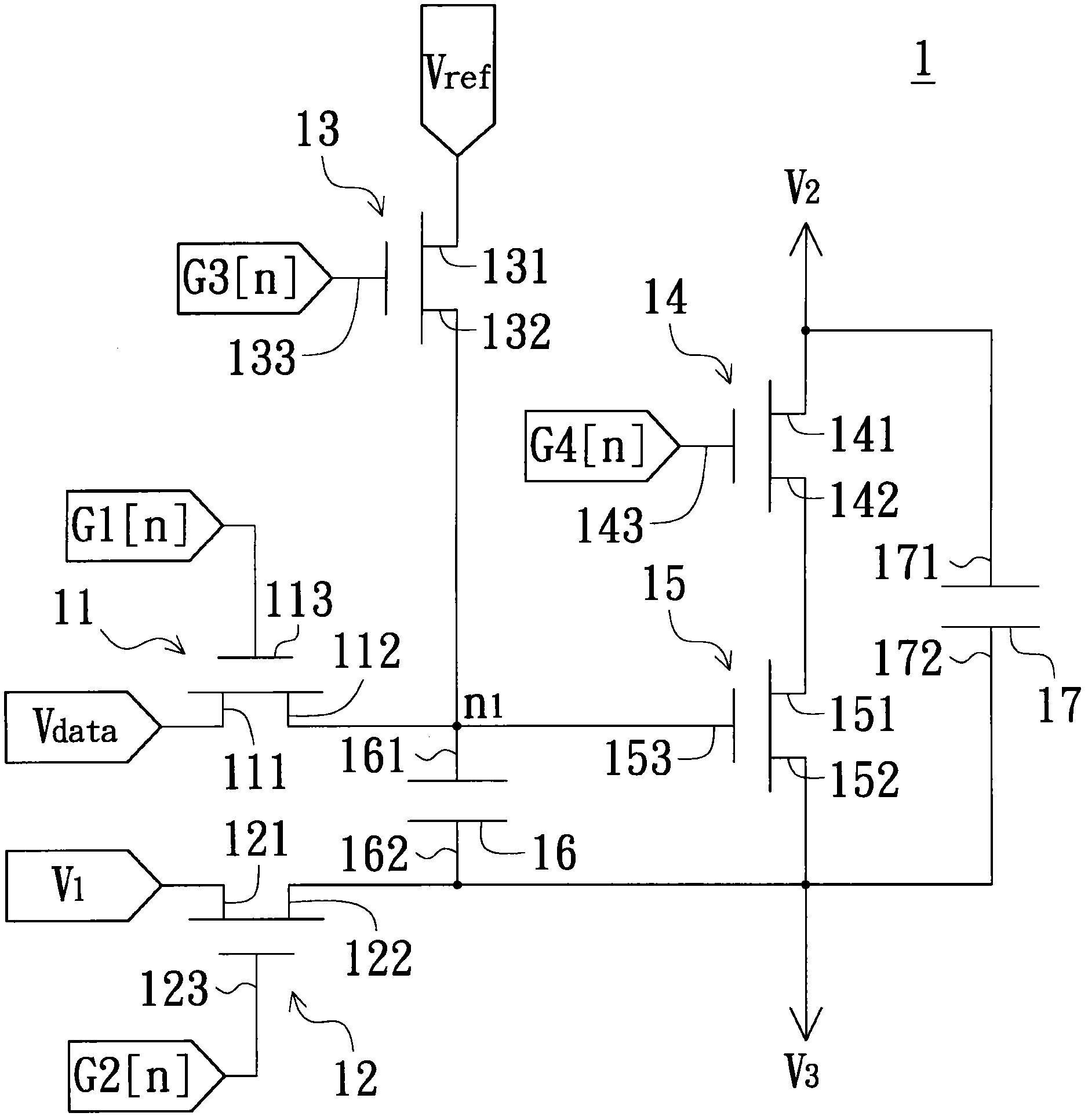
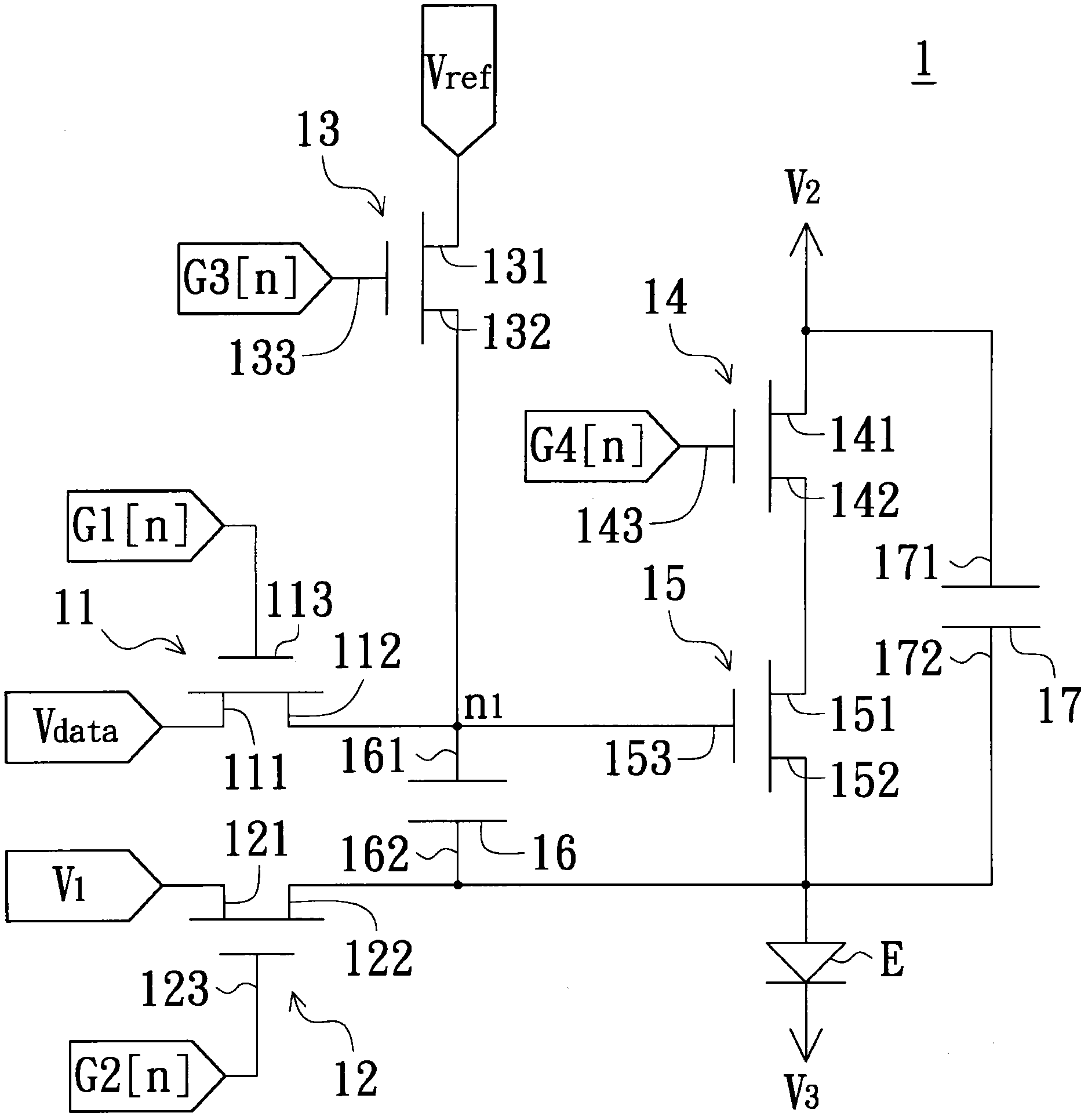
[0055] Such as Figure 2A , is the internal circuit of the pixel circuit of the present invention, wherein the pixel circuit 1 includes a first switch 11, a second switch 12, a third switch 13, a fourth switch 14, a driving transistor 15, a first capacitor 16 and a second capacitor 17, Wherein, each of the switches 11 - 14 and the driving transistor 15 has a first terminal, a second terminal and a control terminal for determining whether the fi...


PUM


Abstract

The invention provides a pixel circuit and a driving method thereof. The pixel circuit comprises five transistors and two capacitors. The drive method comprises the steps of providing three control signals and grid signals to the pixel circuit respectively; adjusting the enabling state of the above control signals and maintaining the grid signals not to be enabled so as to rest the data of the pixel circuit and obtain the voltage compensation effect; enabling the grid signals so as to enable the pixel circuit to be in a data write-in period; and providing the data voltage to the pixel circuit during the data write-in period so as to change the end-point voltage for driving the transistor of a light-emitting element.

Description

technical field [0001] The present invention relates to a pixel circuit circuit and its applied driving method, in particular to a description of a pixel circuit with five transistors and two capacitors and a method for driving the pixel circuit. Background technique [0002] Organic Light Emitting Diode (OLED) can be divided into passive matrix OLED (PMOLED) and active matrix OLED (AMOLED) according to the driving method. PMOLED does not emit light when data is not written, but only emits light during data writing. This driving method has a simple structure, low cost, and is easier to design, and early technicians all developed towards this technology. However, due to the reason of the driving method, the problems of large power consumption and short life are quite serious when developing large-size displays. Mainly used in small and medium size displays. [0003] The biggest difference between AMOLED and PMOLED is that each pixel has a capacitor to store data, so that e...

Claims


Application Information

Patent Timeline
IPC IPC(8): G09G3/32
CPCG09G3/14G09G2300/0852G09G2300/0861G09G3/3233G09G2300/0819
Inventor 蔡宗廷李允翔
Owner AU OPTRONICS CORP
Why Eureka
Try Eureka