
Image sensor and photosensitive diode

A technology of image sensor and photosensitive diode, which is applied in the direction of semiconductor devices, electrical components, circuits, etc., can solve problems such as crosstalk and affecting the performance of image sensors, and achieve the effect of improving quantum efficiency

Inactive Publication Date: 2012-05-02
SHANGHAI HUAHONG GRACE SEMICON MFG CORP
View PDF4 Cites 6 Cited by
  • Summary
  • Abstract
  • Description
  • Claims
  • Application Information

AI Technical Summary

Problems solved by technology

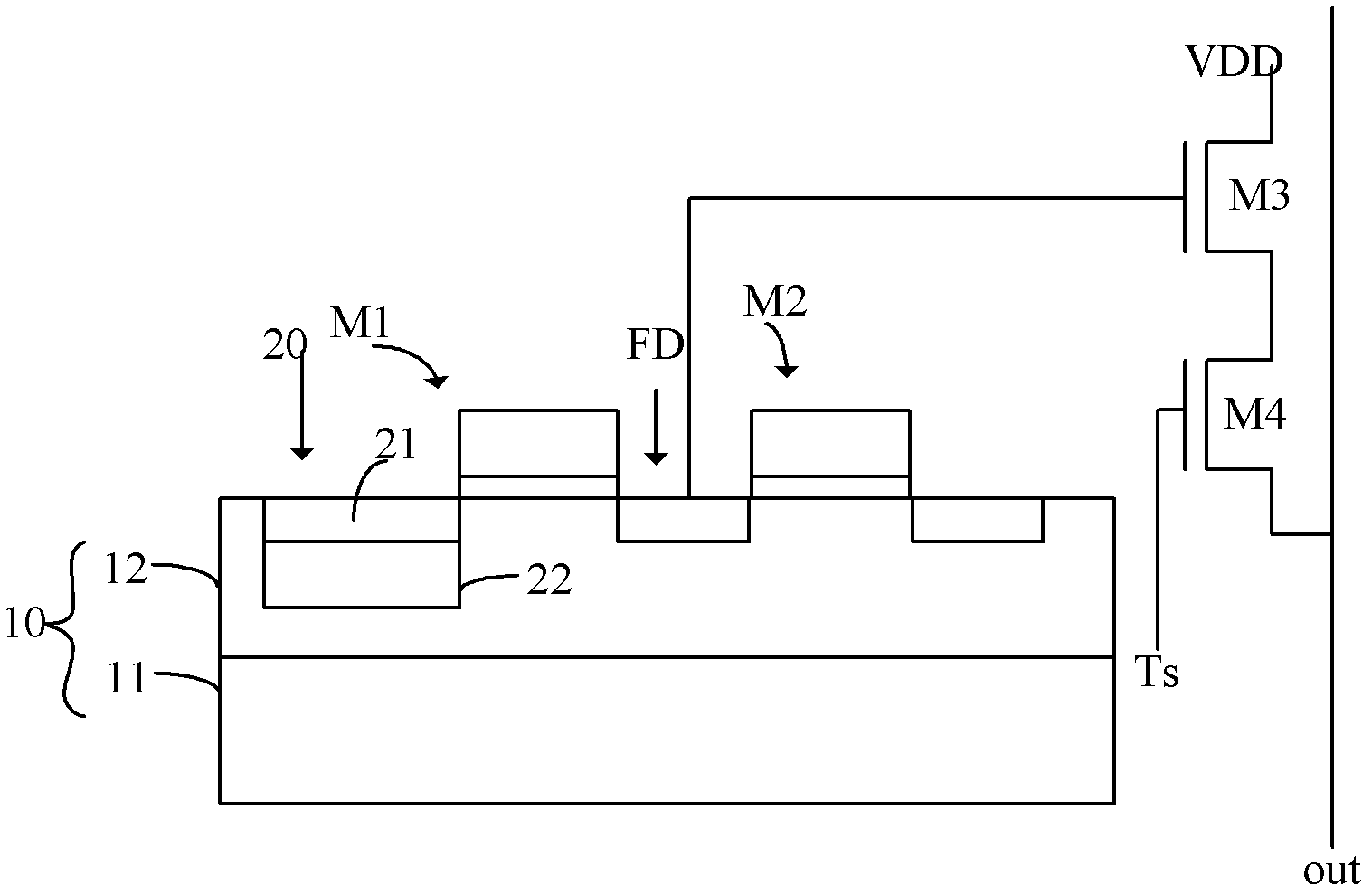
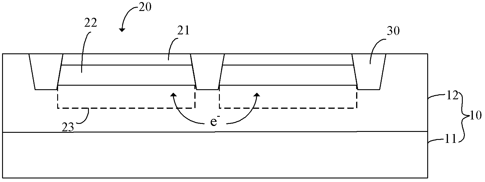
In the prior art image sensor, electronic crosstalk is easily generated between adjacent photodiodes 20, thereby affecting the performance of the image sensor
[0007] In the prior art, there are many patents and patent applications related to CMOS image sensors, such as the Chinese patent application document with the publication number CN1992305A published on July 4, 2007, but none of them solve the above technical problems

Method used


Image

  • Image sensor and photosensitive diode
  • Image sensor and photosensitive diode
  • Image sensor and photosensitive diode

Examples


Embodiment Construction

[0037] In order to make the above objects, features and advantages of the present invention more comprehensible, specific implementations of the present invention will be described in detail below in conjunction with the accompanying drawings.

[0038] In the following description, specific details are set forth in order to provide a thorough understanding of the present invention. However, the present invention can be implemented in many other ways than those described here, and those skilled in the art can make similar extensions without departing from the connotation of the present invention. Accordingly, the present invention is not limited to the specific embodiments disclosed below.

[0039] In the prior art, crosstalk tends to occur between adjacent photodiodes, thereby affecting the performance of the image sensor. refer to figure 2 , the inventor found that in the prior art, when the photosensitive diode is exposed to external light, long-wave light (such as red li...


PUM


Abstract

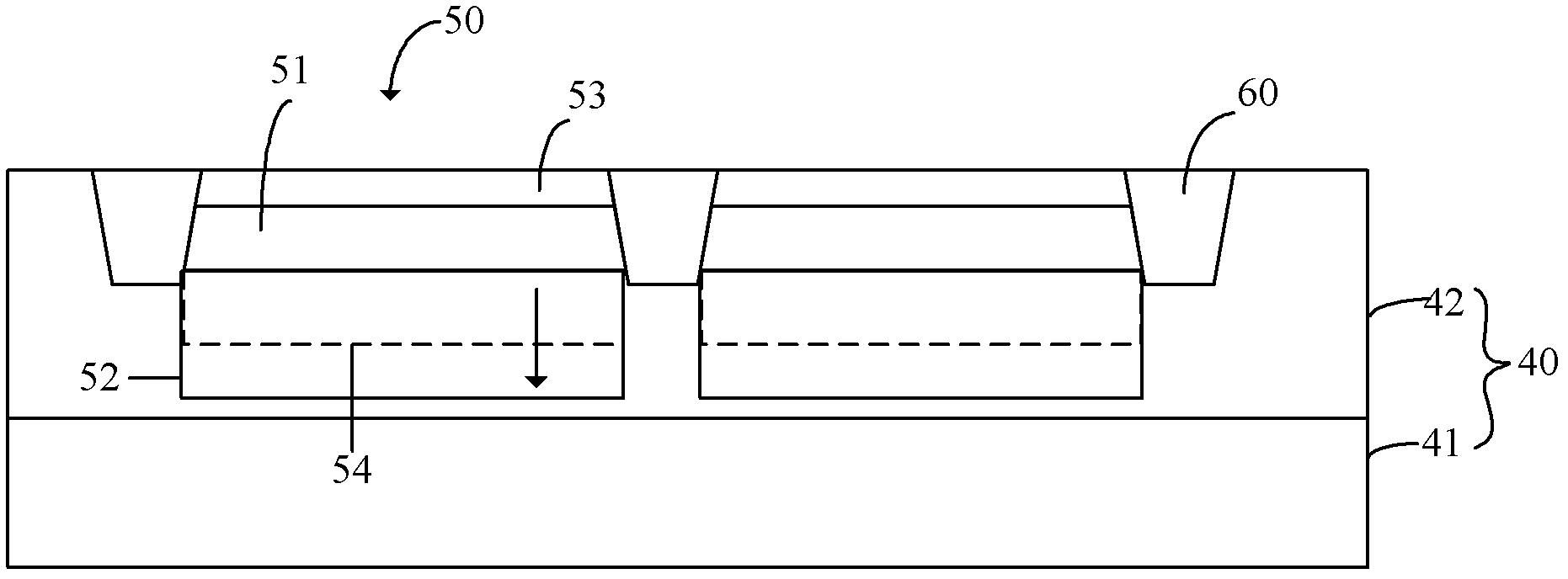
The invention provides a CMOS image sensor and a photosensitive diode. The CMOS image sensor comprises a substrate, an isolation structure and the photosensitive diode. The isolation structure and the photosensitive diode are alternatively provided in the substrate. The photosensitive diode comprises a first doping zone and a second doping zone under the first doping zone. Doping types of the first doping zone and the second doping zone are opposite. Ion doping concentration of the second doping zone in a direction from the first doping zone to the second doping zone is gradually enlarged. According to a technical scheme in the invention, the CMOS image sensor does not have an electrical crosstalk phenomenon, and quantum efficiency of a long wave can be raised.

Description

technical field [0001] The invention relates to the technical field of semiconductors, in particular to photosensitive diodes and CMOS image sensors. Background technique [0002] Image sensors belong to the optoelectronic components in the optoelectronic industry. With the rapid development of digital technology, semiconductor manufacturing technology and the Internet, the market and the industry are now facing the arrival of the era of video, video, and communication integration across various platforms. The beauty of everyday human life in the future. With its application in daily life, it is undoubtedly a digital camera product, and its development speed can be described as changing with each passing day. In just a few years, digital cameras have developed from hundreds of thousands of pixels to 4 million, 5 million pixels or even higher. Not only in developed European and American countries, digital cameras already occupy a large market, but also in developing China, ...

Claims


Application Information

Patent Timeline
Patent Type & Authority Applications(China)
IPC IPC(8): H01L27/146H01L31/103
Inventor 饶金华张克云吴小利
Owner SHANGHAI HUAHONG GRACE SEMICON MFG CORP
Learn More