SiO2/SiN double layer passivation layer T-typed grid AlGaN/GaN HEMT and manufacturing method thereof

A production method and passivation layer technology, which is applied in semiconductor/solid-state device manufacturing, electrical components, circuits, etc., can solve problems such as reducing the current cut-off frequency, and achieve improved current cut-off frequency, good passivation effect, and low gate parasitics The effect of capacitance

Inactive Publication Date: 2012-05-02
INST OF SEMICONDUCTORS - CHINESE ACAD OF SCI
View PDF7 Cites 23 Cited by
  • Summary
  • Abstract
  • Description
  • Claims
  • Application Information

AI Technical Summary

Problems solved by technology

However, in the deep submicron field, due to the high dielectric constant of SiN, the SiN passivation layer increases the parasitic capacitance of the gate, which will significantly reduce the cut-off frequency of the current

Method used


Image

  • SiO2/SiN double layer passivation layer T-typed grid AlGaN/GaN HEMT and manufacturing method thereof
  • SiO2/SiN double layer passivation layer T-typed grid AlGaN/GaN HEMT and manufacturing method thereof
  • SiO2/SiN double layer passivation layer T-typed grid AlGaN/GaN HEMT and manufacturing method thereof

Examples


example

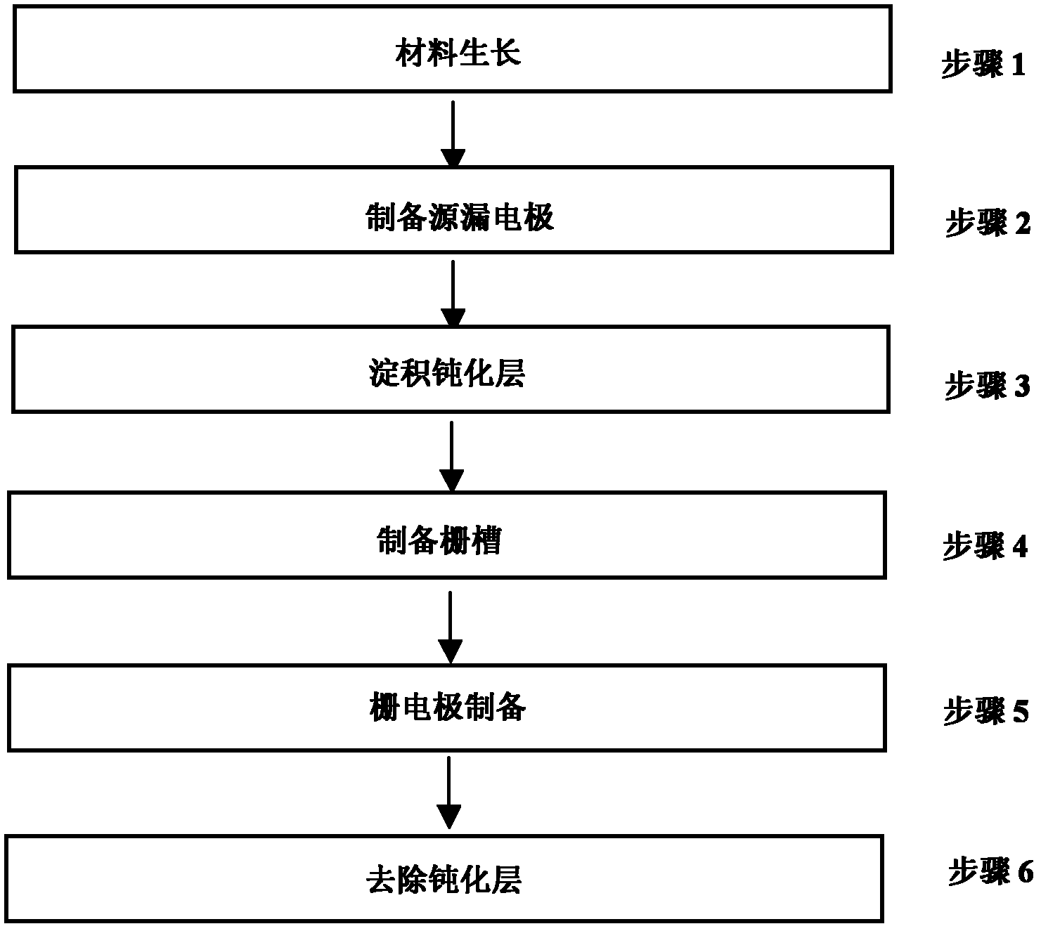
[0043] Referring to Fig. 6, the present invention provides a SiO 2 / SiN double-layer passivated T-gate AlGaN / GaN HEMTs, including:

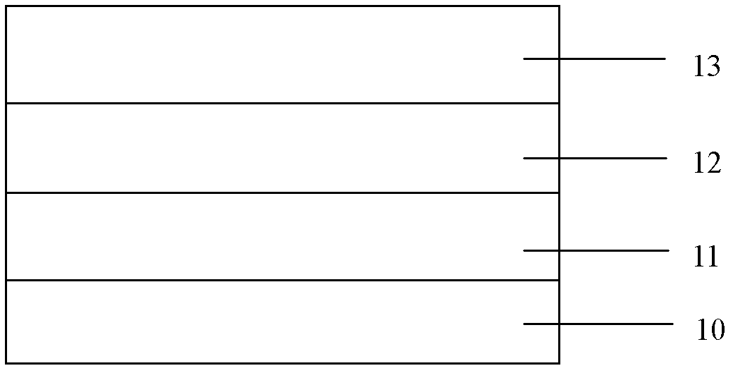
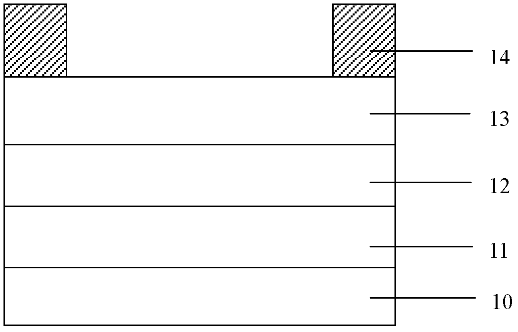
[0044] A substrate 10, on which a GaN buffer layer 11, a GaN intrinsic layer 12 and an Al 0.25 Ga 0.75 N barrier layer 13, the material of the substrate 10 is sapphire;

[0045] A source-drain electrode 14, the source-drain electrode 14 is made on both sides above the barrier layer 13, and the material of the source-drain electrode 14 is Ti / Al / Ni / Au;

[0046] A lower passivation layer 15 is formed between the source and drain electrodes 14 and on the barrier layer 13, the material of the lower passivation layer 15 is SiN, and the thickness is 20nm;

[0047] An upper passivation layer 16 is made between the source and drain electrodes 14 and on the lower passivation layer 15, the material of the upper passivation layer 16 is SiO 2 , with a thickness of 80nm;

[0048] Wherein the middle of the lower passivation layer 15 and the upper passivati...


PUM


Abstract

The invention provides an SiO2/SiN double layer passivation layer T-typed grid AlGaN/GaN HEMT which comprises: a substrate which is grown with a GaN buffer layer, a GaN intrinsic layer and an AlGaN barrier layer in order; source and drain electrodes which are provided on the barrier layer at two sides; a lower passivation layer which is provided between the source and drain electrodes and is on the barrier layer; an upper passivation layer which is provided between the source and drain electrodes and is on the passivation layer, wherein, a bar shaped grid groove is provided between the lower passivation layer and the upper passivation layer; a gate electrode whose section is a T shape, wherein, the gate electrode is provided in the bar shaped grid groove, and an upper part of the gate electrode is higher than a surface of the upper passivation layer.

Description

technical field [0001] The invention relates to the field of manufacturing semiconductor devices, in particular to a SiO 2 / SiN double-layer passivation layer T-type gate AlGaN / GaN HEMT (high electron mobility transistor) and its manufacturing method. Background technique [0002] Microwave power amplifiers are an important part of microwave communication systems such as base stations and satellites. With the rapid development of the wireless communication market, higher requirements are placed on the performance of microwave power amplifier devices, such as high temperature, high frequency, high power, low noise, and high efficiency. Gallium Nitride (GaN), a wide bandgap semiconductor material, is a typical representative of the third-generation semiconductor material. The excellent characteristics of forming high-quality heterostructures are very suitable for the manufacture of high-temperature, high-frequency, high-power, and radiation-resistant microwave electronic dev...

Claims


Application Information

Patent Timeline
Patent Type & Authority Applications(China)
IPC IPC(8): H01L29/778H01L29/423H01L21/335H01L21/28
Inventor 杜彦东韩伟华颜伟张严波杨富华
Owner INST OF SEMICONDUCTORS - CHINESE ACAD OF SCI
Why Eureka
Try Eureka