Laser irradiation apparatus, laser irradiation method, and insulating film forming apparatus

A technology of laser irradiation and laser light source, used in laser parts, laser welding equipment, electrical components, etc., can solve the problems of difficulty in realizing the aperture of the packaging substrate, deterioration of roundness, and failure to achieve practicality.

Inactive Publication Date: 2012-05-09
SUMITOMO HEAVY IND LTD
View PDF9 Cites 36 Cited by
  • Summary
  • Abstract
  • Description
  • Claims
  • Application Information

AI Technical Summary

Problems solved by technology

Therefore, if a solder resist pattern is formed with ink of this drop size, the limit of the hole diameter of the stage (pad) when the surface mount component is mounted on the printed wiring board is about 200 μm, such as Figure 10 As shown in (B), it is difficult to achieve a hole diameter of about 50 μm required for packaging substrates due to deterioration of roundness
Therefore, the practical application of the partial coating method is difficult. At present, the development of a super inkjet with a significantly higher ink discharge volume is currently being developed at the Center of the National Institute of Advanced Industrial Science and Technology, but the goal of practical application has not yet been achieved.

Method used


Image

  • Laser irradiation apparatus, laser irradiation method, and insulating film forming apparatus
  • Laser irradiation apparatus, laser irradiation method, and insulating film forming apparatus
  • Laser irradiation apparatus, laser irradiation method, and insulating film forming apparatus

Examples


Embodiment Construction

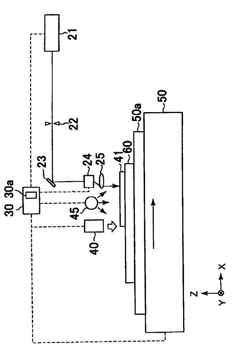
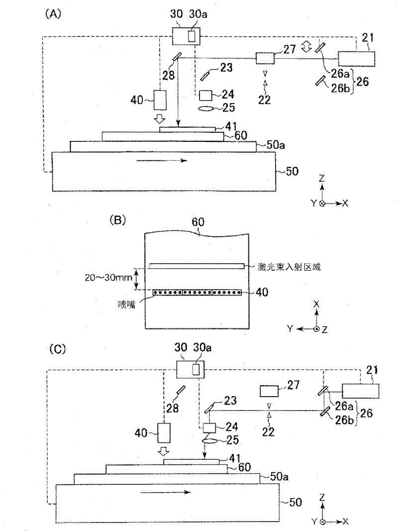
[0035] figure 1 It is a schematic diagram showing the laser irradiation device according to the first embodiment. The laser irradiation device based on the first embodiment includes a laser light source 21, a mask 22, a folding mirror 23, a current scanner 24, an fθ lens 25, a control device 30, an inkjet printer 40, a lamp light source 45, and a stage 50. constitute.

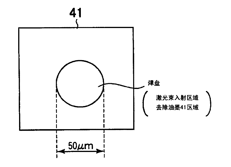
[0036] The control device 30 includes, for example, a storage device 30a as a memory. The stage 50 includes a chuck plate 50 a for sucking and holding a printed wiring board (substrate) 60 as a holding object, and can move the printed wiring board 60 in the in-plane direction. The stage 50 is, for example, an XYθ stage. A solder resist pattern was formed on the printed wiring board 60 held on the stage 50 by the partial coating method using the laser irradiation apparatus according to the first embodiment.

[0037] The stage 50 moves the printed wiring board 60 in the X-axis direction at a constant speed. ...


PUM

PropertyMeasurementUnit
diameteraaaaaaaaaa
thicknessaaaaaaaaaa
pore sizeaaaaaaaaaa

Abstract

The present invention provides a laser irradiation apparatus, a laser irradiation method and an insulating film forming apparatus, wherein a resist pattern is formed with high quality. The laser irradiating apparatus of the invention is provided with the following components: a laser source which sends out pulse laser beam; an object table which holds a substrate; a coating device which coats resist material on the substrate that is held on the object table; a first transmission optical system which focuses the pulse laser beam that is transmitted from the laser source on the resist material that is coated through the coating device for transmission and solidifying the resist material on the transmission position; a second transmission optical system which transmits the pulse laser beam that is sent out from the laser source to the resist material that is solidified by the pulse laser beam that is transmitted through the first transmission optical system and removes the resist material at a transmission position; and an optical path switching device which causes the pulse laser beam that is sent out from the laser source to selectively transmit to the first transmission optical system or the second transmission optical system.

Description

technical field [0001] This application claims priority based on Japanese Patent Application No. 2010-227721 filed on October 7, 2010. The entire content of the application is incorporated in this specification by reference. [0002] The present invention relates to an apparatus and method for irradiating laser beams and an apparatus for forming an insulating film. Background technique [0003] Soldering resist is used to solder the printed wiring board on which the conductor wiring is formed on the base material, exposing the necessary conductor (copper foil) part, and forming on the wiring in such a way that the solder does not adhere to the part that does not need to be soldered. insulating film on the board. [0004] As a method of forming a solder resist pattern on a printed wiring board, for example, the following method is known. First, in order to improve the adhesiveness of the solder resist, the printed wiring board is polished. Next, a resist material is appli...

Claims


Application Information

Patent Timeline
Patent Type & Authority Applications(China)
IPC IPC(8): B23K26/36B23K26/42H05K3/28B23K26/00H05K3/00
CPCH01L2924/0002H01L2924/00H01S3/02H05K3/28
Inventor 礒圭二
Owner SUMITOMO HEAVY IND LTD
Why Eureka
Try Eureka