MOS (Metal Oxide Semiconductor) transistor and manufacturing method thereof

A technology of MOS transistors and manufacturing methods, applied in the field of MOS transistors and their manufacturing, capable of solving problems affecting transistor channel mobility, junction capacitance and junction leakage current, etc.

Active Publication Date: 2012-05-09
SEMICON MFG INT (SHANGHAI) CORP +1
View PDF6 Cites 0 Cited by
  • Summary
  • Abstract
  • Description
  • Claims
  • Application Information

AI Technical Summary

Problems solved by technology

[0010] It has been found in practice that the MOS transistors produced by existing methods have a strong transient enhanced diffusion effect (Transistent Enhanced Diffusion, TED), which not only causes the short channel effect (Short Channel effect, SCE) of the transistor ) and reverse short channel effect (Reverse Short Channel Effect, RSCE), and affect the transistor channel mobility, junction capacitance and junction leakage current

Method used


Image

  • MOS (Metal Oxide Semiconductor) transistor and manufacturing method thereof
  • MOS (Metal Oxide Semiconductor) transistor and manufacturing method thereof
  • MOS (Metal Oxide Semiconductor) transistor and manufacturing method thereof

Examples


Embodiment Construction

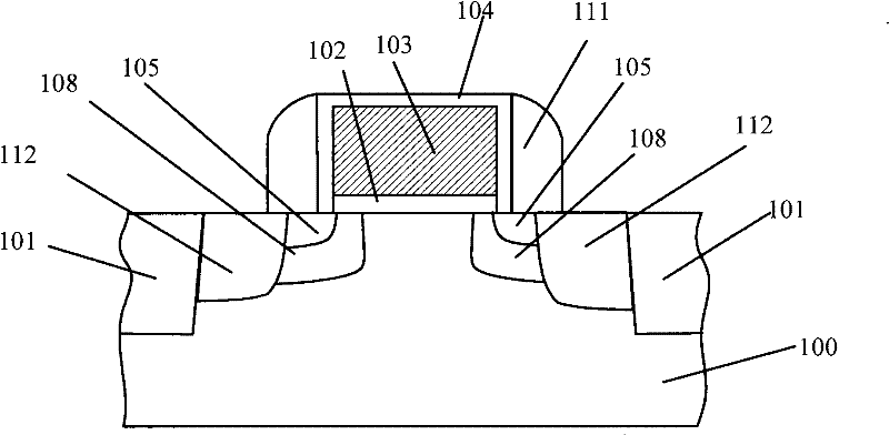
[0043] The inventors found that in the prior art method for forming a MOS transistor, before forming the source / drain extension region and the pocket-shaped implant region, an oxidation process is performed to form an oxide layer on the periphery of the gate structure to protect the gate, but the The oxidation process can form defects in the semiconductor substrate, which are caused by the Oxidation-Enhanced Diffusion (OED) effect. Defects caused by the oxidation-enhanced diffusion effect will diffuse in the subsequent annealing process, causing the dopant ions in the source / drain extension region and the pocket implant region to diffuse, causing a transient enhancement effect and causing a short-channel effect of the device and anti-short channel effects.

[0044] After research, the inventors found that if an oxide layer is formed on the periphery of the gate structure, ion implantation is performed in the pocket implantation area to form a defect adsorption area surrounding...


PUM


Abstract

The invention provides a manufacturing method of a MOS (Metal Oxide Semiconductor) transistor; the manufacturing method comprises the following steps of: providing a semiconductor substrate, and forming a grid structure on the semiconductor substrate; carrying out an oxidation technology to form an oxide layer covering the grid structure; carrying out ion implantation on the semiconductor substrate at the two sides of the grid structure to form source/drain extension regions, pocket implantation regions surrounding the source/drain extension regions and defect adsorption regions surrounding the pocket implantation regions; carrying out an annealing technology, and activating doping ions of the source/drain extension regions, the defect adsorption regions and the pocket implantation regions; forming side walls at the two sides of the grid structure; and by using the grid structure and the side walls as masking films, carrying out source/drain ion implantation, and forming the source/drain regions in the semiconductor substrate at the two sides of the grid structure. According to the manufacturing method, the problem that the doping ions of the pocket implantation regions and the source/drain extension regions diffuse along with defects is solved, the oxidation-enhanced diffusion effect is eliminated, the transient-enhanced diffusion effect is suppressed, and the leakage current of devices is reduced.

Description

technical field [0001] The invention relates to the field of semiconductors, in particular to a MOS transistor and a manufacturing method thereof. Background technique [0002] Metal-oxide-semiconductor (MOS) transistors are the most basic devices in semiconductor manufacturing. They are widely used in various integrated circuits. According to the main carrier and the type of doping during manufacturing, they are divided into NMOS and PMOS transistors. [0003] The prior art provides a method for manufacturing a MOS transistor. Please refer to Figure 1 to Figure 3 , is a schematic cross-sectional structure diagram of a manufacturing method of a MOS transistor in the prior art. [0004] Please refer to figure 1 , providing a semiconductor substrate 100, forming isolation structures 101 in the semiconductor substrate 100, the semiconductor substrate 100 between the isolation structures 101 is an active region, and forming a doped well in the active region (not shown), the...

Claims


Application Information

Patent Timeline
Patent Type & Authority Applications(China)
IPC IPC(8): H01L21/336H01L29/78H01L29/06
Inventor 赵猛
Owner SEMICON MFG INT (SHANGHAI) CORP
Why Eureka
Try Eureka