High-dielectric-constant gate dielectric material and preparation method thereof

A high dielectric constant, gate dielectric technology, applied in metal material coating process, circuits, electrical components, etc., can solve the problem of difficult to form a continuous crystalline structure, and achieve the solution of crystallization, high k value, and large band gap. Effect

Inactive Publication Date: 2012-05-16
INST OF MICROELECTRONICS CHINESE ACAD OF SCI
View PDF1 Cites 5 Cited by
  • Summary
  • Abstract
  • Description
  • Claims
  • Application Information

AI Technical Summary

Problems solved by technology

[0005] On the other hand, with the further reduction of the feature size of MOS devices, the thickness of the gate dielectric film is required to be higher, and for ultra-thin films (such as 1-3nm), it is generally difficult to form a continuous crystalline structure in existing processes. The crystallization of thin films is also one of the problems to be solved

Method used


Image

  • High-dielectric-constant gate dielectric material and preparation method thereof
  • High-dielectric-constant gate dielectric material and preparation method thereof
  • High-dielectric-constant gate dielectric material and preparation method thereof

Examples


preparation example Construction

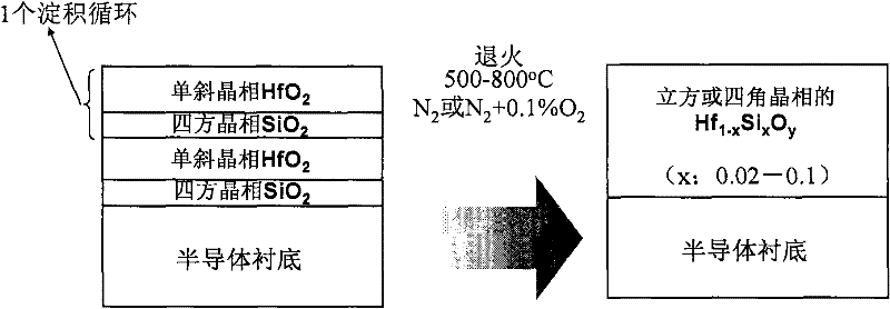
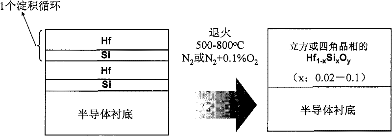
[0025] The following will be combined with Figure 2-4 Describe in detail the gate dielectric material Hf 1-x Si x o y The preparation method comprises the following steps: depositing material A containing Hf source and material B containing Si source or material C containing Hf source and Si source through a film-forming process; then performing thermal annealing, The annealing temperature is 500-800°C to form Hf with cubic or tetragonal crystal phase 1-x Si x o y For thin films, x ranges from 0.02-0.1. Among them, the optimum annealing temperature is 650-800°C; the annealing time is 5-300s, and the optimum is 20-120s; the annealing atmosphere is N 2 or O 2 The volume content is 0.1%-1% N 2 +O 2 The combination.

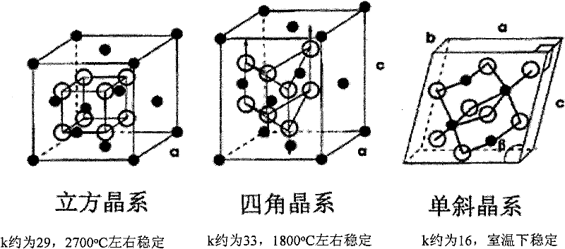
[0026] It should be pointed out that if Hf 1-x Si x o y If the Si content is not high enough, it is difficult to use the annealing process to make HfSiO with amorphous or monoclinic phase structure z Transform into cubic or tetragonal crystal phase, if...

Embodiment 1

[0028] Embodiment one (PVD film formation):

[0029] First use PVD method to deposit and form a film, the process pressure can be 0.2-1Pa, the sputtering atmosphere can be Ar gas, the flow rate can be 15-50sccm, the temperature range of the semiconductor substrate can be room temperature-400°C, and then at 500-800°C temperature, N 2 Or contain 1% (volume ratio) O 2 N 2 +O 2 Annealed in an annealing atmosphere to form Hf with cubic or tetragonal phase 1-x Si x o y film. Among them, the film forming methods include the following two types:

[0030] Method 1: co-sputtering targets of material A containing Hf source and material B containing Si source, or sputtering targets of material C containing Hf source and Si source, to form an amorphous substrate on the semiconductor substrate phase or monoclinic phase of Hf 1-x Si x o y film. Specifically, materials A and B can be single substance materials such as Hf and Si, or HfO 2 and SiO 2 and other binary oxides, the ma...

Embodiment 2

[0032] Embodiment two (MOCVD or ALD film formation):

[0033] First, use MOCVD or ALD method to deposit and form a film, the temperature of the reaction chamber is 200-600°C, and then at 2 Or contain 1% (volume ratio) O 2 N 2 +O 2 Annealed in an annealing atmosphere to form Hf with cubic or tetragonal phase 1-x Si x o y film. Among them, the film forming methods include the following two types:

[0034] Mode 1: The material A containing Hf source and the material B containing Si source are introduced into the reaction chamber at the same time, so as to form Hf in amorphous phase or monoclinic phase on the semiconductor substrate. 1-x Si x o y film. Specifically, material A includes an organometallic source Hf(N(CH 3 ) 2 ) 4 (TMDEAH), Hf(NC 2 h 5 CH 3 ) 4 (TEMAH), Hf(N(C 2 h 5 ) 2 ) 4 (TDEAH) or inorganic metal source HfCl 4 Any one or a combination of them, material B includes organic source C 8 h 22 N 2 Si(SAM24), HSi[N(CH 3 ) 2 ] 3 (3DMAS) in any ...


PUM

PropertyMeasurementUnit
relative permittivityaaaaaaaaaa

Abstract

The invention discloses a high-dielectric-constant gate dielectric material and a preparation method thereof. The preparation method comprises the following steps of: doping SiO2 components with certain amount into a high k gate dielectric material HfO2 to form Hf1-xSixOy with a cubic crystal phase or a quadrilateral crystal phase in combination with an optimized thermal treatment process, and thus obtaining a high k gate dielectric film material with a larger gap, a higher k value and thermal stability. In addition, a high k gate dielectric film and a formation method thereof contribute to solving the problem of crystallization of ultra-thin films.

Description

technical field [0001] The invention relates to the field of semiconductor material and its preparation, in particular to a gate dielectric material with high dielectric constant and its preparation method. Background technique [0002] High-k gate dielectric materials have been widely concerned and applied in the CMOS (Complementary Metal Oxide Semiconductor) process, especially in the technology generation of 45nm and below. The introduction of a high-k gate dielectric material can ensure that the physical thickness of the gate dielectric can be effectively increased under the same equivalent oxide thickness (EOT), so that the purpose of suppressing gate leakage current can be achieved. HfO 2 It is currently considered to be one of the high-k gate dielectric materials most likely to be applied to the CMOS process. HfO 2 The relative permittivity k value is between 16-25, the band gap is about 5.8eV, and the conduction band offset is about 1.4eV. These electrical propert...

Claims


Application Information

Patent Timeline
Patent Type & Authority Applications(China)
IPC IPC(8): C23C14/08C23C14/58C23C16/40C23C16/56H01L29/51
CPCC23C14/08C23C16/40C23C16/401C23C16/56C23C14/5806H01L29/51C23C14/58
Inventor 王文武赵超马雪丽陈大鹏
Owner INST OF MICROELECTRONICS CHINESE ACAD OF SCI
Why Eureka
Try Eureka