High-K gate dielectric layer formation method and semiconductor device

A gate dielectric layer and semiconductor technology, applied in semiconductor devices, semiconductor/solid-state device manufacturing, electrical components, etc., can solve the problems of thick equivalent oxide layer, poor film quality, instability, etc., and achieve thin equivalent Thickness of oxide layer, high K value, effect of increasing K value

Inactive Publication Date: 2016-02-03
SEMICON MFG INT (SHANGHAI) CORP
View PDF4 Cites 1 Cited by
  • Summary
  • Abstract
  • Description
  • Claims
  • Application Information

AI Technical Summary

Problems solved by technology

However, using ZrO 2 Has the following disadvantages: at higher processing temperatures ZrO 2 not stable with silicon
[0008] However, the high-K gate dielectric layer formed by the above method has many disadvantages, such as poor film quality and thick equivalent oxide thickness (EOT) due to its insufficient K value.

Method used


Image

  • High-K gate dielectric layer formation method and semiconductor device
  • High-K gate dielectric layer formation method and semiconductor device
  • High-K gate dielectric layer formation method and semiconductor device

Examples


Embodiment Construction

[0041] The present invention will be further described below with reference to specific embodiments and drawings, but the protection scope of the present invention should not be limited by this.

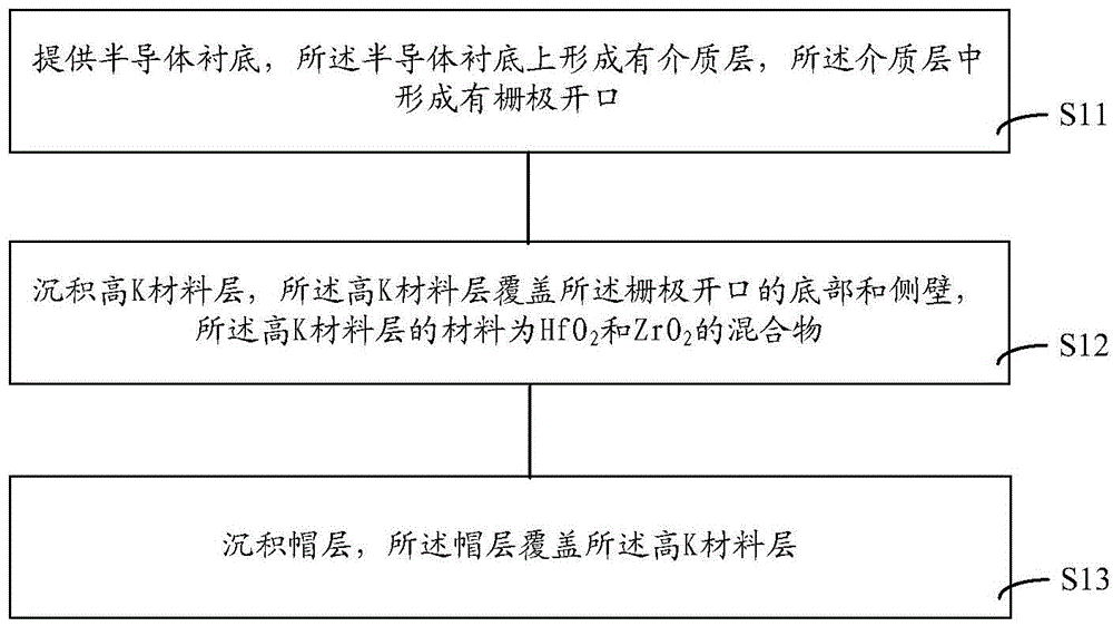
[0042] reference image 3 The method for forming the high-K gate dielectric layer of this embodiment includes the following steps:

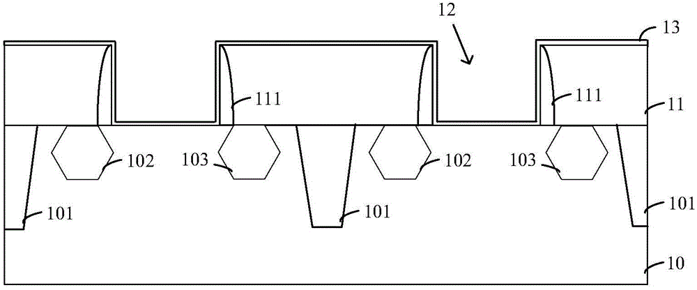
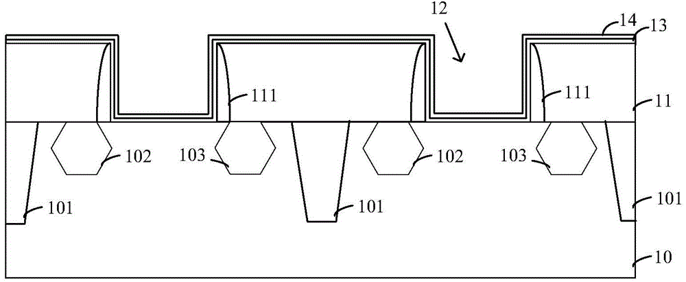
[0043] Step S11, providing a semiconductor substrate, a dielectric layer is formed on the semiconductor substrate, and a gate opening is formed in the dielectric layer;

[0044] Step S12, deposit a high-K material layer, the high-K material layer covers the bottom and sidewalls of the gate opening, and the material of the high-K material layer is HfO 2 And ZrO 2 mixture;

[0045] Step S13, depositing a cap layer, the cap layer covering the high-K material layer.

[0046] Combine below Figure 4 to Figure 13 Give details.

[0047] reference Figure 4 A semiconductor substrate 20 is provided, and a dummy gate 204 is formed on the semiconductor substrate 20, and a sp...


PUM


Abstract

The invention provides a high-K gate dielectric layer formation method and a semiconductor device. The method comprises the following steps: providing a semiconductor substrate, a dielectric layer being formed on the semiconductor substrate, and a gate opening being formed in the dielectric layer; and depositing a high-K material layer, wherein the high-K material layer covers the bottom portion and side wall of the gate opening, and the high-K material layer is made of the mixture of HfO2 and ZrO2. The method helps to improve the film quality of a high-K gate dielectric layer, and helps to form the high-K gate dielectric layer having higher K value and thinner equivalent oxide layer thickness.

Description

Technical field [0001] The invention relates to a semiconductor device and semiconductor process technology, in particular to a method for forming a high-K gate dielectric layer and a semiconductor device. Background technique [0002] When the high-k gate dielectric metal gate process (HKMG) first appeared, ZrO 2 Because of its high dielectric constant (K) and low transition temperature from amorphous to crystalline, it has received extensive attention. However, using ZrO 2 It has the following disadvantages: ZrO at higher processing temperature 2 It is not stable with silicon. [0003] HfO 2 The dielectric constant is about 20, and it is refractory enough under normal silicon processing conditions and will not react with the silicon substrate or the polysilicon electrode on it. Therefore, the existing technology currently usually uses HfO 2 To form a high-K gate dielectric layer. [0004] figure 1 with figure 2 The formation process of a high-K gate dielectric layer in the prior...

Claims


Application Information

Patent Timeline
Patent Type & Authority Applications(China)
IPC IPC(8): H01L21/28H01L21/283H01L29/51
Inventor 库尔班·阿吾提
Owner SEMICON MFG INT (SHANGHAI) CORP
Why Eureka
Try Eureka