Electrostatic discharge protection circuit

A technology for electrostatic discharge and protection of equipment, applied in the field of circuits, which can solve problems such as insufficient holding voltage, latch failure, large chip area, etc.

Active Publication Date: 2012-05-16
TAIWAN SEMICON MFG CO LTD
View PDF6 Cites 17 Cited by
  • Summary
  • Abstract
  • Description
  • Claims
  • Application Information

AI Technical Summary

Problems solved by technology

However, with the development of submicron semiconductor technology, the existing ESD protection schemes can no longer meet the growing needs of the semiconductor industry
For example, in high-voltage applications, SCR or NMOS-based ESD protection circuits can cause latch failure due to insufficient holding voltage
On the other hand, even with a relatively high hold voltage, an RC-triggered PMOS transistor takes up a large chip area

Method used


Image

  • Electrostatic discharge protection circuit
  • Electrostatic discharge protection circuit
  • Electrostatic discharge protection circuit

Examples


Embodiment Construction

[0035] The construction and use of the presently preferred embodiments are discussed in detail below. It should be appreciated, however, that the present invention provides many useful inventive concepts that can be implemented in a wide variety of specific contexts. The specific embodiments discussed are merely examples of specific ways to make and use the invention, and do not limit the scope of the invention.

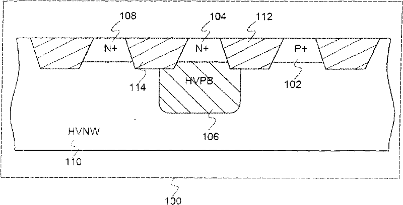
[0036] figure 1 A simplified cross-sectional view of an ESD protection structure 100 according to one embodiment is shown. The ESD protection structure 100 includes a P+ region 102, a first N+ region 104, a second N+ region 108, a first isolation region 112, a second isolation region 114, a high voltage P-type implant region 106 and a high voltage N well (HVNW) 110 . The first N+ region 104 and the high voltage P-type implant region 106 are sequentially disposed on the HVNW 110 . The high voltage P-type implantation region 106 is disposed under the first N+ regio...


PUM


Abstract

An electrostatic discharge (ESD) protection structure comprises a high voltage P type implanted region disposed underneath an N+ region. The high voltage P type implanted region and the N+ region form a reverse diode or a Zener diode depending on different doping densities. The ESD protection structure further comprises a plurality of P+ and N+ regions. The high voltage P type implanted region and the P+ and N+ regions form a semiconductor device having a breakdown characteristic. In one embodiment, the semiconductor device may be a bipolar PNP transistor. The bipolar PNP transistor and a Zener diode in series connection form an ESD protection circuit. In another embodiment, the semiconductor device may be a Silicon-Controlled Rectifier (SCR), which is series-connected with a reverse diode. Both embodiments provide a reliable ESD protection.

Description

technical field [0001] The present invention relates to the field of circuits, and more specifically, to an electrostatic discharge protection circuit. Background technique [0002] Electrostatic discharge (ESD) is a rapid electrical discharge that flows between two objects due to the build-up of electrostatic charge. Because of the relatively large currents generated by this rapid discharge, ESD can burn out semiconductor devices. In order to reduce semiconductor damage caused by ESD, ESD protection circuits have been developed to provide current discharge paths. When an ESD event occurs, the discharge current is conducted through the discharge path instead of passing through the protected internal circuit. [0003] In semiconductor technology, NMOS transistors, silicon controlled rectifiers (SCRs) and RC-triggered PMOS transistors are widely used. However, with the development of submicron semiconductor technology, the existing ESD protection schemes can no longer meet ...

Claims


Application Information

Patent Timeline
Patent Type & Authority Applications(China)
IPC IPC(8): H01L27/02H01L29/06H01L29/74
CPCH01L27/0262H01L29/87H01L27/0259H01L27/0248
Inventor 黄新言
Owner TAIWAN SEMICON MFG CO LTD
Why Eureka
Try Eureka