Display device and method for manufacturing the same

一种显示装置、制造方法的技术,应用在半导体/固态器件制造、光学、仪器等方向,能够解决不容易增加显示装置开口率等问题,达到减少步骤的效果

Active Publication Date: 2012-05-16
SAMSUNG DISPLAY CO LTD
View PDF4 Cites 10 Cited by
  • Summary
  • Abstract
  • Description
  • Claims
  • Application Information

AI Technical Summary

Problems solved by technology

In simplifying the entire manufacturing process of display devices, the process for forming the ohmic contact layer becomes a limitation
[0004] In addition, since capacitors generally include at least one metal electrode, it is not easy to increase the aperture ratio of the display device

Method used


Image

  • Display device and method for manufacturing the same
  • Display device and method for manufacturing the same
  • Display device and method for manufacturing the same

Examples


Embodiment Construction

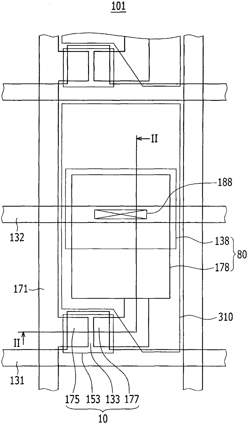
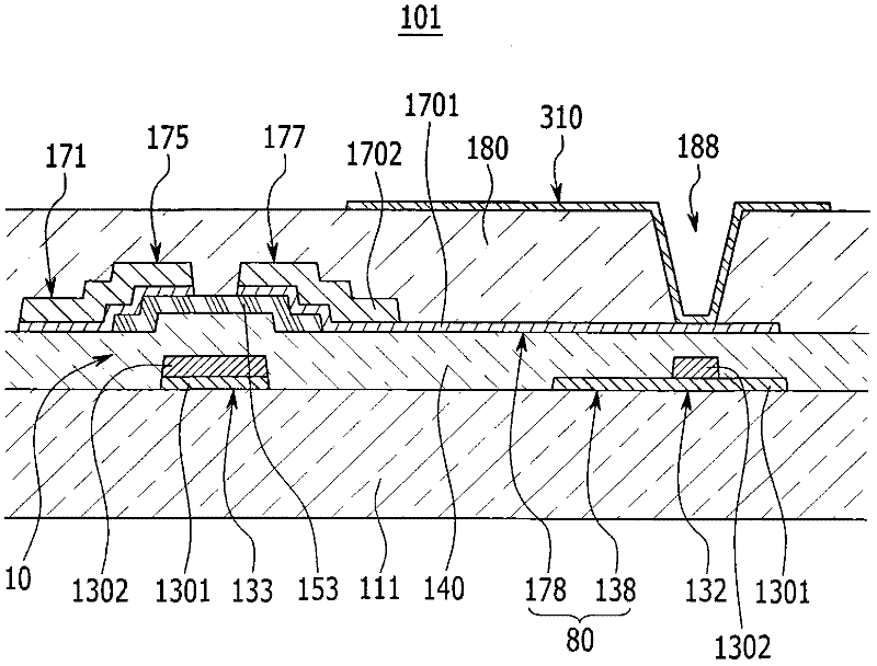
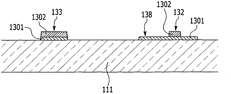
[0046] The present invention will be described more fully with reference to the accompanying drawings, in which exemplary embodiments of the invention are shown. As those skilled in the art would realize, the described embodiments may be modified in various different ways, all without departing from the spirit or scope of the present invention.

[0047] Throughout the specification, the same reference numerals refer to the same constituent elements. Among several exemplary embodiments, in exemplary embodiments other than the first exemplary embodiment, elements different from those of the first exemplary embodiment will be described in more detail.

[0048] Further, the size and thickness of each element shown in the drawings are described for better understanding and ease of description, and the present invention is not limited to the described size and thickness.

[0049] In the drawings, the thickness of layers, films, panels, regions, etc., are exaggerated for clarity. I...


PUM


Abstract

A display device according to an exemplary embodiment includes: gate wires, at least one of the gate wires having a first multi-layered structure including a first transparent conductive layer formed on the substrate and a first metal layer formed on the first transparent conductive layer and at least another one of the gate wires having a first single-layered structure formed with the first transparent conductive layer; a semiconductor layer formed on a part of the gate wires; and data wires with at least one of the data wires having a second multi-layered structure including a second transparent conductive layer formed on the semiconductor layer and a second metal layer formed on the second transparent conductive layer and at least another one of the data wires having a second single-layered structure formed with the second transparent conductive layer.

Description

technical field [0001] Exemplary embodiments of the described technology relate to display devices and methods of manufacturing the same. More specifically, the described technology relates to a display device and a method of manufacturing the same while simplifying its structure while increasing its aperture ratio. Background technique [0002] Most flat panel display devices, such as organic light emitting diode (OLED) displays, liquid crystal displays (LCD), etc., include thin film transistors and capacitors. [0003] A thin film transistor includes an ohmic contact layer formed to reduce contact resistance between a semiconductor layer and source and drain electrodes. The ohmic contact layer is often formed by doping the semiconductor layer with impurities. In simplifying the entire manufacturing process of a display device, a process for forming an ohmic contact layer becomes a limitation. [0004] In addition, since the capacitor generally includes at least one meta...

Claims


Application Information

Patent Timeline
Patent Type & Authority Applications(China)
IPC IPC(8): H01L27/12G02F1/1362G02F1/1368H01L21/77H01L27/32
CPCH01L27/3262G02F1/136213H01L27/1225H01L27/3265H01L29/4908H01L27/1255H01L27/124G02F1/136227H10K59/1213H10K59/1216H10K59/131
Inventor 权珉圣尹柱善
Owner SAMSUNG DISPLAY CO LTD
Why Eureka
Try Eureka