Semiconductor structure and manufacture method thereof

A manufacturing method and semiconductor technology, applied in semiconductor/solid-state device manufacturing, semiconductor devices, electrical components, etc., can solve problems such as unfavorable short channel effects

Inactive Publication Date: 2012-05-16
UNITED MICROELECTRONICS CORP
View PDF5 Cites 3 Cited by
  • Summary
  • Abstract
  • Description
  • Claims
  • Application Information

AI Technical Summary

Problems solved by technology

Although the recessed source and drain regions of this specific shape can further increase the stress on the gate channel, it may also be due to the back-diffusion of dopants in the doped epitaxial layer, such as boron, into the gate channel. adverse short channel effect

Method used


Image

  • Semiconductor structure and manufacture method thereof
  • Semiconductor structure and manufacture method thereof
  • Semiconductor structure and manufacture method thereof

Examples


Embodiment Construction

[0043] The invention provides a semiconductor structure and a manufacturing method thereof. The semiconductor structure of the present invention has a non-doped epitaxial layer close to the cavity and used as a buffer layer. These non-doped epitaxial layers can isolate the back diffusion of dopants in the doped epitaxial layer. In addition, the non-doped epitaxial layers have appropriate thicknesses, so the stress generated by the doped epitaxial layers will not be affected.

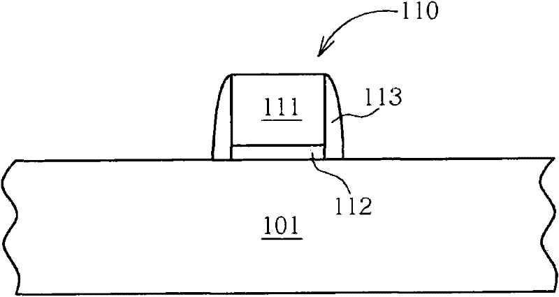
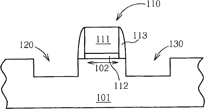
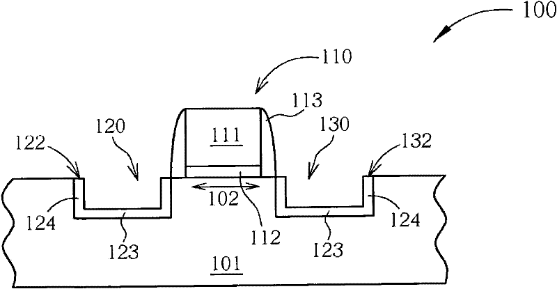
[0044] The present invention firstly provides a method for manufacturing a semiconductor structure. Figure 1-Figure 5 A schematic flow chart illustrating a method for fabricating a semiconductor structure of the present invention. Please refer to figure 1 , first provide a substrate 101 . The substrate 101 is usually a semiconductor substrate, such as silicon with a single crystal structure. Next, a gate structure 110 is formed on the substrate 101 . The required gate structure 110 can be formed o...


PUM


Abstract

The invention discloses a semiconductor structure and a manufacture method thereof. The semiconductor structure comprises a recess in base material, a non-doped epitaxial layer and a doped epitaxial layer. The non-doped epitaxial layer is on an internal surface of the recess and is composed of silicon and epitaxial material essentially. The non-doped epitaxial layer covers a bottom and a sidewall of the internal surface of the recess, and thickness of the bottom is not larger than 120% of thickness of the sidewall. The non-doped epitaxial layer and the doped epitaxial layer fill the recess together.

Description

technical field [0001] The invention relates to a composite epitaxial layer structure and a method for forming the composite epitaxial layer structure. In particular, the present invention relates to a composite epitaxial layer structure comprising a non-doped epitaxial layer and a doped epitaxial layer, and a method for forming the composite epitaxial layer structure, so as to ensure the electrical stability of the gate channel. Background technique [0002] In the manufacturing process of semiconductor devices, it is always a challenge for those skilled in the art to continue to reduce critical dimensions while maintaining the performance of semiconductor devices. One of the challenges is to maintain sufficient carrier mobility in the gate channel, namely electrons and holes. It is known that as long as proper stress is applied to the gate channel, the mobility of carriers in the gate channel of metal oxide semiconductors, such as N-MOS or P-MOS, can be adjusted. One way...

Claims


Application Information

Patent Timeline
Patent Type & Authority Applications(China)
IPC IPC(8): H01L29/78H01L29/06H01L21/336H01L21/20
Inventor 廖晋毅李静宜詹书俨
Owner UNITED MICROELECTRONICS CORP
Why Eureka
Try Eureka