Microwave plasma source and plasma processing apparatus

A microwave plasma and plasma technology, applied in the direction of plasma, semiconductor/solid-state device manufacturing, discharge tube, etc., can solve problems such as trouble

Inactive Publication Date: 2012-05-16
TOKYO ELECTRON LTD
View PDF9 Cites 9 Cited by
  • Summary
  • Abstract
  • Description
  • Claims
  • Application Information

AI Technical Summary

Problems solved by technology

[0005] In such an RLSA microwave plasma device, when adjusting the plasma distribution, it is necessary to prepare multiple antennas with different slot shapes and patterns, and it is necessary to exchange antennas, which is very troublesome.

Method used


Image

  • Microwave plasma source and plasma processing apparatus
  • Microwave plasma source and plasma processing apparatus
  • Microwave plasma source and plasma processing apparatus

Examples


no. 1 approach

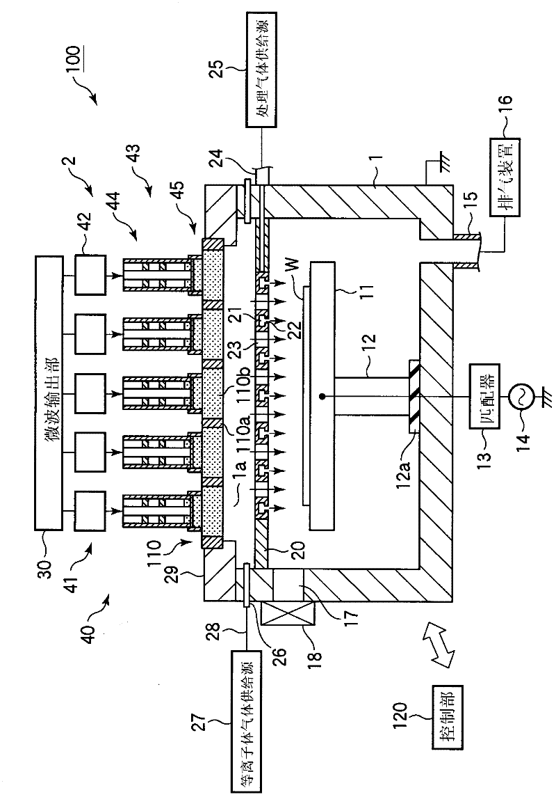
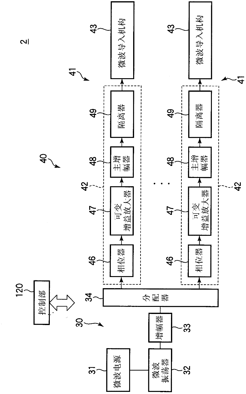
[0059] figure 1 is a cross-sectional view showing a schematic structure of a surface wave plasma processing apparatus having a microwave plasma source according to a first embodiment of the present invention, figure 2 is a structural diagram showing the structure of a microwave plasma source, image 3 It is a plan view schematically showing the microwave supply part of the microwave plasma source, Figure 4 is a diagram showing an example of a circuit configuration of a main amplifier used in an antenna module in a microwave plasma source, Figure 5 A sectional view showing the microwave introducing mechanism used in the antenna module of the microwave plasma source, Image 6 In order to represent the power supply structure of the microwave introduction mechanism, in Figure 5 A cross-sectional view of the AA' line, Figure 7 To represent the iron core and sliding parts in the tuner, in Figure 5 A cross-sectional view of the BB' line.

[0060] The surface wave plasma pro...

no. 2 approach

[0110] Next, a second embodiment of the present invention will be described.

[0111] In this embodiment, the basic structure of the microwave plasma source and the plasma processing device is the same as that of the first embodiment, and the structure of the top plate is different.

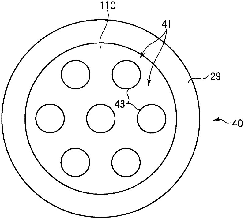
[0112] Figure 12 It is a plan view schematically showing the microwave supply part and the top plate of the plasma source in this embodiment, Figure 13 for in Figure 12 Cross-sectional view of line CC'. As shown in these figures, in this embodiment, a circular top plate 110 is formed, and a dielectric member 110b made of a dielectric such as quartz is embedded in a portion where a plurality of microwave introduction mechanisms 43 for radiating microwaves into the chamber 1 are arranged. It has a hexagonal shape, and between adjacent dielectric members 110b, one side of the hexagonal shape is provided close to each other so as to face each other. Therefore, in the metal frame 110a supportin...


PUM


Abstract

There are provided a microwave plasma source and a plasma processing apparatus capable of improving uniformity of a plasma density distribution within a processing chamber by controlling positions of nodes and antinodes of a standing wave of microwave within the processing chamber not to be fixed. The microwave plasma source 2 includes a microwave supply unit 40. The microwave supply unit 40 includes multiple microwave introducing devices 43 each introducing microwave into the processing chamber; and multiple phase controllers 46 for adjusting phases of the microwaves inputted to the microwave introducing devices 43. Here, the phases of the microwaves inputted to the microwave introducing devices 43 are adjusted by fixing an input phase of the microwave inputted to one of two adjacent microwave introducing devices 43 while varying an input phase of the microwave inputted to the other microwave introducing device 43 according to a periodic waveform.

Description

technical field [0001] The present invention relates to a microwave plasma source and a plasma processing device using the same. Background technique [0002] In the manufacturing process of semiconductor devices and liquid crystal display devices, in order to perform plasma processing such as etching or film formation on substrates such as semiconductor wafers and glass substrates, plasma etching equipment or plasma CVD film formation equipment is used. and other plasma processing equipment. [0003] Recently, as such a plasma processing apparatus, an RLSA (Radial Line Slot Antenna) microwave plasma processing apparatus capable of uniformly forming surface wave plasma with a high density and a low electron temperature has attracted attention (for example, Patent Document 1). [0004] The RLSA microwave plasma processing device is equipped with a planar antenna (Radial Line Slot Antenna) with slots formed in a predetermined pattern on the upper part of the chamber (processi...

Claims


Application Information

Patent Timeline
Patent Type & Authority Applications(China)
IPC IPC(8): H05H1/46
CPCH01J37/32293H05H2001/463H05H1/46H05H1/463H01L21/3065H01L21/205
Inventor 池田太郎长田勇辉
Owner TOKYO ELECTRON LTD
Why Eureka
Try Eureka