Maskless lithography device

A maskless lithography and lithography technology, applied in the field of microelectronics, can solve the problem of inability to achieve precise adjustment of the distance between the focusing diffractive optical element and the substrate, and achieve the effects of simple structure, low cost and high focusing precision

Inactive Publication Date: 2012-05-30
INST OF MICROELECTRONICS CHINESE ACAD OF SCI
View PDF2 Cites 2 Cited by
  • Summary
  • Abstract
  • Description
  • Claims
  • Application Information

AI Technical Summary

Problems solved by technology

[0004] In the process of realizing the present invention, the inventor realized that the existing technology has the following defects: when using the maskless lithography, the precise adjustment of the distance between the focusing diffractive optical element and the substrate cannot be realized.

Method used


Image

  • Maskless lithography device
  • Maskless lithography device
  • Maskless lithography device

Examples


Embodiment Construction

[0020] In order to make the object, technical solution and advantages of the present invention clearer, the present invention will be described in further detail below in conjunction with specific embodiments and with reference to the accompanying drawings.

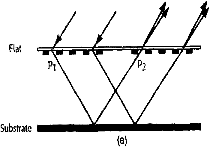
[0021] The present invention provides a maskless lithography apparatus, comprising a focusing diffractive optical element for mapping a preset lithographic pattern to a substrate; a first moiré grating group located on a plane where the focusing diffractive optical element is located above, including at least two moiré gratings, for adjusting the distance between the focusing diffractive optical element and the substrate by utilizing the movement of the moiré fringes generated by the moiré gratings. The focusing diffractive optical element and the focusing assembly are formed by etching a light-transmitting substrate coated with an opaque metal film. Preferably, the focusing diffractive optical element and the first moiré...


PUM

PropertyMeasurementUnit
widthaaaaaaaaaa

Abstract

The invention discloses a maskless lithography device comprising a focus diffractive optical element and a first Moire grating group, wherein the focus diffractive optical element is used for transferring a preset lithography graph to a substrate; and the first Moire grating group is positioned on a plane on which the focus diffractive optical element is positioned, comprises at least two Moire gratings, and is used for adjusting the distance between the focus diffractive optical element and the substrate by utilizing the movement of Moire patterns generated by the at least two Moire gratings. The maskless lithography device provided by the invention is used for integrating the Moire grating group for focusing and the focus diffractive optical element together, and has the advantages of high focusing accuracy, simple structure and low cost.

Description

technical field [0001] The invention relates to the technical field of microelectronics, in particular to a maskless photolithography device. Background technique [0002] Diffractive optical elements are a general term for elements that use the diffraction phenomenon of light to modulate the wavefront of light waves to achieve specific optical functions. Diffractive optical elements include various gratings, zone plates, photonic sieves, etc. They have been widely used in spectroscopy, wavefront shaping, optical communication, focusing imaging, microfabrication and other fields. [0003] Zone plate and photon sieve are diffractive optical elements with self-focusing ability. Among them, the zone plate is composed of transparent and opaque rings alternately. Block the odd-numbered or even-numbered bands in the Fresnel half-wave band, and under the illumination of a point light source, it can be focused to obtain a high-intensity image point. The resolution of a zone plat...

Claims


Application Information

Patent Timeline
Patent Type & Authority Applications(China)
IPC IPC(8): G03F7/207G02B5/18
Inventor 谢常青潘一鸣朱效立刘明
Owner INST OF MICROELECTRONICS CHINESE ACAD OF SCI
Why Eureka
Try Eureka