Antenna device
An antenna device, antenna element technology, applied in the direction of antenna, antenna support/mounting device, antenna coupling, etc., to achieve reliable detection effect
- Summary
- Abstract
- Description
- Claims
- Application Information
AI Technical Summary
Problems solved by technology
Method used
Image
Examples
no. 1 Embodiment approach
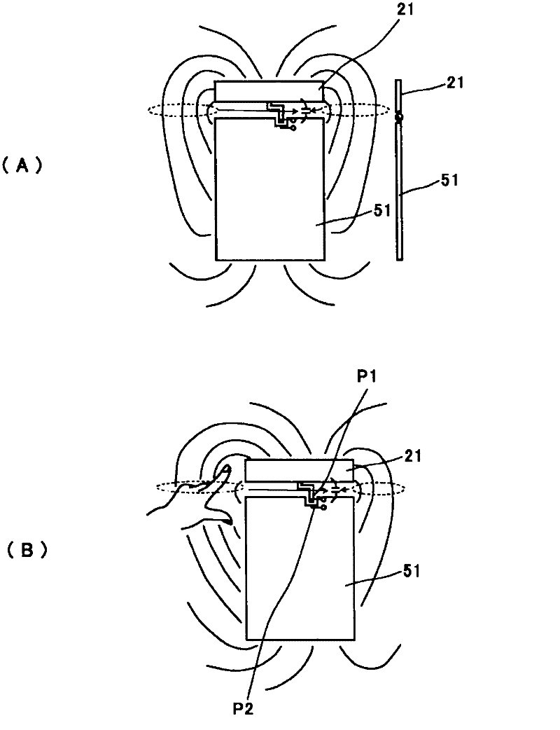
[0056] refer to Figure 2 to Figure 7 The antenna device according to the first embodiment will be described.
[0057] Between the antenna element electrode 21 and the ground electrode 51 of the substrate, as figure 2 An electric field is formed as schematically represented by lines of force in (A). For high frequencies such as wireless communication signals, electromagnetic waves are radiated to the outside by the electric field described above appearing alternately. For direct current, however, a so-called electrostatic field is formed.
[0058] exist figure 2 The right side of (A) shows that a pseudo dipole is constituted by the antenna element electrode 21 and the ground electrode 51 of the substrate.
[0059] The antenna element electrode 21 and the ground electrode 51 of the substrate can be regarded as opposing conductors in a capacitor connected by the above-mentioned electric force line, and this capacitance is a so-called parasitic capacitance that determines t...
no. 2 Embodiment approach
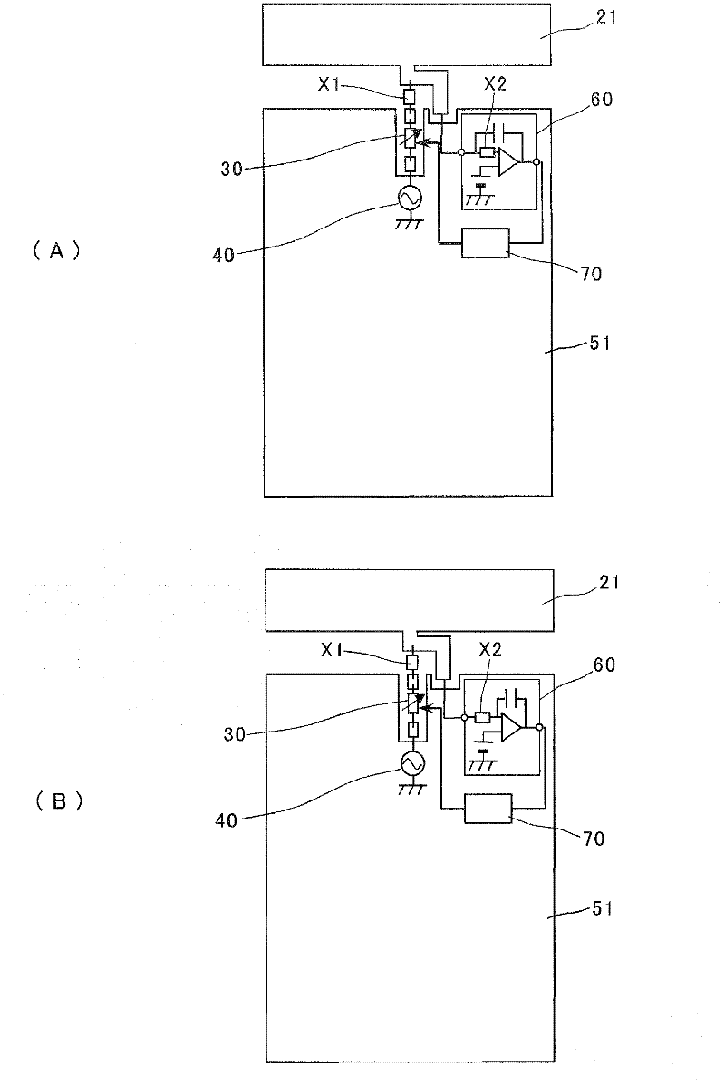
[0095] In the second embodiment, the reactance element provided in the wireless communication signal path that is the propagation path between the antenna element and the power supply unit, and the sensing signal path that is the propagation path between the antenna element and the capacitance detection circuit are shown. A specific example of the reactance element provided in .
[0096] Figure 8 It is a diagram showing two configurations of the antenna device according to the second embodiment.
[0097] exist Figure 8 In (A), the capacitor C is provided in the wireless communication signal path PW1 that is a propagation path between the antenna element electrode 21 and the feeding circuit 40 . Furthermore, an inductor L is provided in the sensing signal path PW2 which is a propagation path between the antenna element electrode 21 and the capacitance detection circuit 60 .
[0098] exist Figure 8 In (A), although the capacitor C provided in the wireless communication si...
no. 3 Embodiment approach
[0105] In the third embodiment, a specific configuration example of the capacitance detection circuit is shown.
[0106] Figure 10 (A) is a circuit diagram showing a capacitance detection circuit provided in the antenna device according to the third embodiment, Figure 10 (B) is a waveform diagram showing its operation.
[0107] Here, an operational amplifier is used based on two viewpoints of taking out an output signal as a voltage signal and amplifying it. The capacitance-voltage conversion circuit is composed of an inverting amplifier circuit based on an operational amplifier OP1, a detection target capacitance Cs, and a feedback capacitance Cf. A reference potential Vref1 is applied to the non-inverting input terminal of the operational amplifier OP1. The operation principle of this capacitance-voltage conversion circuit is to amplify a changing voltage (V=Q / C) caused by the movement of charge between Cs-Cf due to the capacitance change of the detection target capacit...
PUM
 Abstract
Description
Claims
Application Information
 - R&D
- Intellectual Property
- Life Sciences
- Materials
- Tech Scout
- Unparalleled Data Quality
- Higher Quality Content
- 60% Fewer Hallucinations
Browse by: Latest US Patents, China's latest patents, Technical Efficacy Thesaurus, Application Domain, Technology Topic, Popular Technical Reports.
© 2025 PatSnap. All rights reserved.Legal|Privacy policy|Modern Slavery Act Transparency Statement|Sitemap|About US| Contact US: help@patsnap.com


