Wafer cleaning device and method

A technology for cleaning devices and wafers, applied in cleaning methods and appliances, chemical instruments and methods, electrical components, etc., can solve problems affecting wafer quality, affecting work efficiency, and scratches on the surface of wafer 10, etc., to achieve extended The effect of improving service life, improving work efficiency and improving cleaning effect

Inactive Publication Date: 2012-06-06
SEMICONDUCTOR MANUFACTURING INTERNATIONAL (BEIJING) CORP +1
View PDF4 Cites 14 Cited by
  • Summary
  • Abstract
  • Description
  • Claims
  • Application Information

AI Technical Summary

Problems solved by technology

[0005] Then, in the prior art, due to the long-term use of the cleaning equipment, the following problems will occur: the cleaning brush 20 is stained with dirt for a long time, such as including organic residues and surface particles, and the dirt stays on the cleaning brush. In the case of continuous opera

Method used


Image

  • Wafer cleaning device and method
  • Wafer cleaning device and method
  • Wafer cleaning device and method

Examples


Embodiment Construction

[0024] In order to make the content of the present invention clearer and easier to understand, the content of the present invention will be further described below in conjunction with the accompanying drawings. Of course, the present invention is not limited to this specific embodiment, and general replacements known to those skilled in the art are also covered within the protection scope of the present invention.

[0025] Secondly, the present invention is described in detail by means of schematic diagrams. When describing the examples of the present invention in detail, for the convenience of explanation, the schematic diagrams are not partially enlarged according to the general scale, which should not be used as a limitation of the present invention.

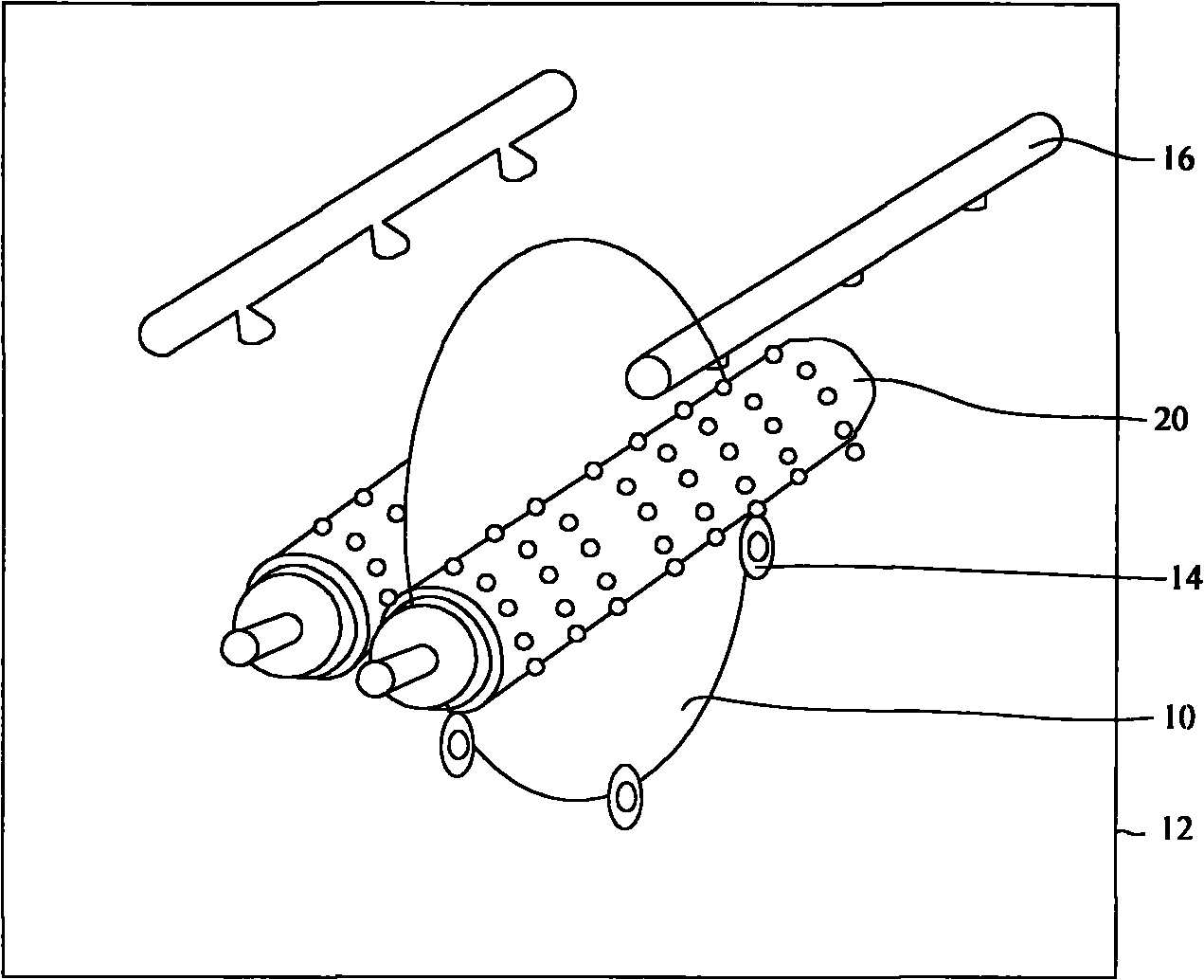
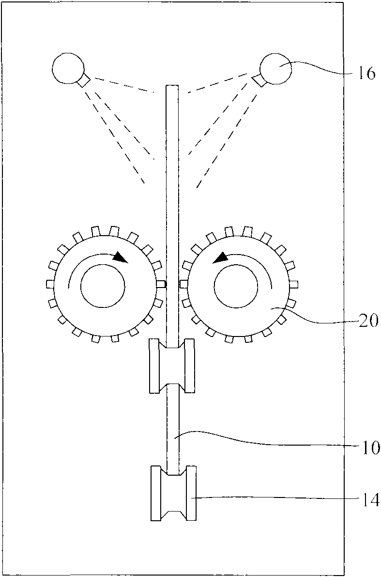
[0026] image 3 It is a structural schematic diagram of an embodiment of the wafer cleaning device of the present invention. like image 3 As shown, the present invention provides a wafer cleaning device, comprising:

[00...


PUM


Abstract

The invention provides a wafer cleaning device which comprises a cleaning trough, a wafer rotating device, a spray tube and a cleaning mechanism, wherein the wafer rotating device is configured in the cleaning trough and used to fix and drive a wafer to be cleaned to rotate; the spray tube comprises a plurality of nozzles and is configured in the cleaning trough and positioned above the wafer to be cleaned; the cleaning mechanism is positioned on the side of the wafer to be cleaned and comprises a loading mechanism and cleaning brushes; and the loading mechanism is provided with at least two cleaning brushes, and the cleaning brushes can alternately clean the wafer to be cleaned. The wafer cleaning device provided by the invention can realize multi-channel cleaning technical mode, namely that a plurality of cleaning brushes can be arranged in one cleaning device, and the cleaning brushes alternately clean the wafer in the cleaning process, thus under the condition of not affecting the cleaning process, the wafer to be cleaned can be brushed and washed and the cleaning brushes can be cleaned. Therefore, the cleaning effect of the cleaning brushes can be increased, the working efficiency can be increased, and the service life of the cleaning brushes can be prolonged.

Description

technical field [0001] The invention relates to a semiconductor manufacturing process, in particular to a wafer cleaning device and method thereof. Background technique [0002] Chemical Mechanical Polishing (CMP) technology is a combination of mechanical grinding and chemical corrosion. Chemical mechanical polishing technology uses the grinding effect of ultra-fine particles and the chemical corrosion of slurry to form a smooth and flat surface on the surface of the ground medium. plane. Chemical mechanical polishing technology is the product of the development of integrated circuits (IC) towards miniaturization, multilayering, thinning, and planarization. It has become the mainstream technology in the semiconductor manufacturing industry. It is a necessary process technology to improve production efficiency, reduce manufacturing cost and planarize the substrate globally. Chemical mechanical polishing technology has become the central technology of semiconductor manufactu...

Claims


Application Information

Patent Timeline
IPC IPC(8): B08B7/04H01L21/02
Inventor 沙酉鹤彭名君
Owner SEMICONDUCTOR MANUFACTURING INTERNATIONAL (BEIJING) CORP
Why Eureka
Try Eureka