Method for removing residual polymers from protecting layer of semiconductor device

A protective layer, polymer technology, applied in semiconductor/solid-state device manufacturing, cleaning methods using liquids, chemical instruments and methods, etc., can solve problems such as collapse and enlargement of protective layers

Inactive Publication Date: 2012-06-06
SEMICON MFG INT (SHANGHAI) CORP +1
View PDF2 Cites 1 Cited by
  • Summary
  • Abstract
  • Description
  • Claims
  • Application Information

AI Technical Summary

Problems solved by technology

However, as the feature size of the semiconductor device decreases, the aspect ratio of the protective layer with the protective layer pattern is also increased. If the ultrasonic method or further etching of the protective layer is used to completely remove the etching residue on the sidewall of the protective layer , the pressure will be exerted on the protective layer with the protective layer pattern, and the pressure on the protective layer with the protective layer pattern will gradually increase as the feature size gradually decreases, eventually leading to the collapse of the protective layer

Method used


Image

  • Method for removing residual polymers from protecting layer of semiconductor device
  • Method for removing residual polymers from protecting layer of semiconductor device
  • Method for removing residual polymers from protecting layer of semiconductor device

Examples


Embodiment Construction

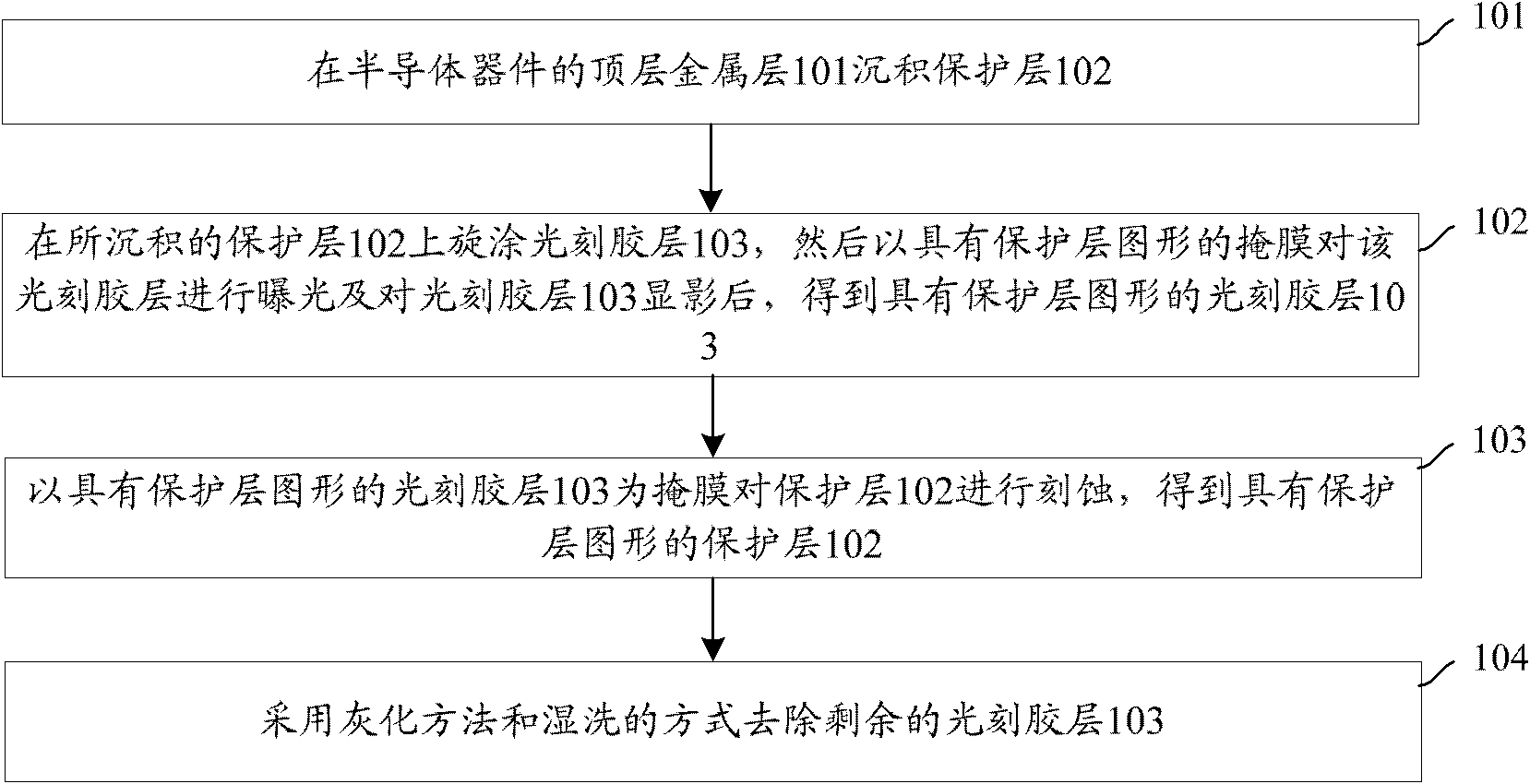
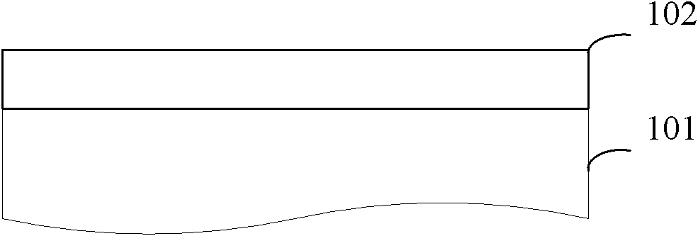
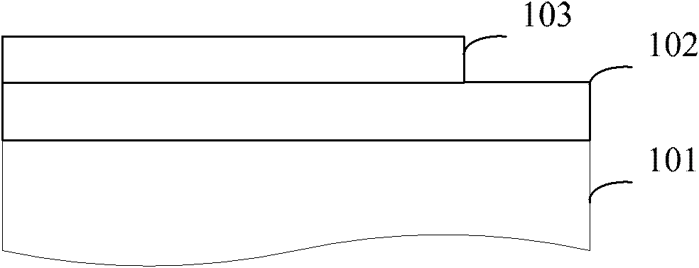
[0031] In order to make the object, technical solution and advantages of the present invention clearer, the present invention will be further described in detail below with reference to the accompanying drawings and examples.

[0032] It can be seen from the prior art that in the process of completely removing the etching residual polymer of the protective layer, the reason for the collapse of the protective layer is that the ultrasonic method or the method of further etching the protective layer will directly act on the surface of the protective layer, making the protective layer The surface pressure increases or damages the surface of the protective layer, resulting in the collapse of the protective layer with an increasing aspect ratio.

[0033] In order to overcome the above problems, the present invention proposes to use deionized water spray cleaning method to remove the etching residue of the protective layer, such as only for the place where there is etching residual po...


PUM


Abstract

The invention discloses a method for removing residual polymers from a protecting layer of a semiconductor device. The method comprises the following steps of: after depositing the protecting layer on a top metal layer of the semiconductor device, coating a photoresist layer; carrying out exposure and development on the photoresist layer in sequence by using a mask with a protecting layer graphic, and obtaining the photoresist layer with a protecting layer; etching the protecting layer by using the photoresist layer with the protecting layer with a protecting layer graphic as a mask, obtaining the protecting layer with the protecting layer graphic and remaining the polymers on the protecting layer; and adopting ashing and wet cleaning modes to remove the remaining photoresist layer and adopting a deionized-water spraying mode to remove the residual polymers. According to the method, the residual polymers on the protecting layer of the semiconductor device can be completely removed on the premise that the protecting layer is ensured not to be collapsed.

Description

technical field [0001] The invention relates to the field of semiconductor manufacturing, in particular to a method for removing residual polymers in a protective layer of a semiconductor device. Background technique [0002] In the final stage of the semiconductor manufacturing process, after the top metal layer of the semiconductor device is fabricated, that is, after the pad metal is formed on the top dielectric layer, it is necessary to deposit a protective layer and etch the deposited protective layer to expose the pad. Solder joint metal, and finally get the semiconductor device. After the parameter test of the final semiconductor device is passed, the chip can be packaged. [0003] At present, the flow chart of a method for depositing a protective layer on the top metal layer of a semiconductor device and etching the deposited protective layer is as follows: figure 1 shown, refer to Figure 2a-2d The shown schematic cross-sectional view of depositing a protective l...

Claims


Application Information

Patent Timeline
IPC IPC(8): H01L21/02B08B3/02
Inventor 秦伟张校平代大全吴森
Owner SEMICON MFG INT (SHANGHAI) CORP
Why Eureka
Try Eureka