Testing method of COG (chip on glass) product of PMOLED (passive matrix organic light emitting diode) based on tape carrier package

A technology of product testing and thin-film packaging, which is applied in the field of PMOLED COG product testing, can solve the problems of low substrate utilization, high testing cost, processing accuracy and cutting alignment accuracy, and achieve low cost and convenient testing.

Inactive Publication Date: 2014-02-12
SICHUAN CCO DISPLAY TECH
View PDF3 Cites 0 Cited by
  • Summary
  • Abstract
  • Description
  • Claims
  • Application Information

AI Technical Summary

Problems solved by technology

[0004] The technical problem to be solved by the present invention is to propose a method for testing COG products based on thin-film-encapsulated PMOLEDs, which solves the problem of low substrate utilization caused by the test method of COF products in the traditional technology and the high cost of testing and the existence of processing problems caused by the test method of COG products. The problem of precision and cutting alignment accuracy

Method used


Image

  • Testing method of COG (chip on glass) product of PMOLED (passive matrix organic light emitting diode) based on tape carrier package

Examples


Embodiment Construction

[0008] The present invention will be further described below in conjunction with the accompanying drawings.

[0009] Aiming at the low utilization rate of the substrate caused by the test method of COF products in the traditional technology and the high test cost caused by the test method of COG products, there are problems of processing accuracy and cutting alignment accuracy, the present invention proposes a COG product test based on thin-film packaged PMOLED Method, this test method comprises two big steps: 1. the making step of test point; 2. test step;

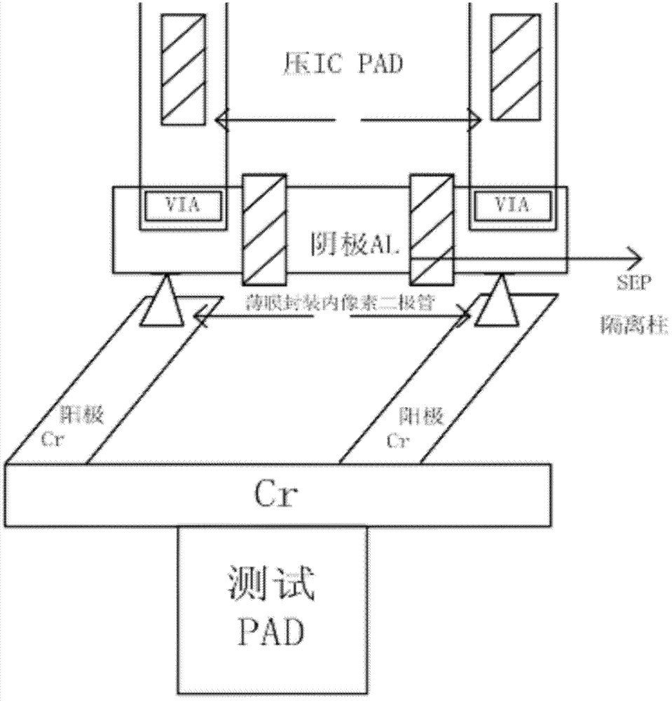
[0010] see figure 1 , the production process of the test point (test PAD) is as follows: set a diode at each IC pin, and divide the metal Cr on the screen used to connect the IC pin (press IC PAD) into three sections functionally: A piece of metal Cr is used to connect the anode of the diode, and a via (VIA) is made on the second piece of metal Cr, so that the voltage on the cathode of the diode can be transmitted to the...


PUM


Abstract

The invention relates to a testing technology of a PMOLED (passive matrix organic light emitting diode), discloses a testing method of a COG (chip on glass) product of a PMOLED based on taper carrier package, and aims at solving the problems of low utilization rate of a substrate caused by a testing mode of a COF (chip on flex) product in the traditional technology, as well as high test cost, low processing precision and cut alignment precision caused by the testing method of the COG product. The method is characterized in that: a diode is arranged at each IC (integrated circuit) pin, and is used for dividing metal Cr on a screen of the IC pin into three sections, wherein the first section of metal Cr is used for connecting an anode end of the diode, the second section of metal Cr is provided with a through hole, and the third section of metal Cr is connected with the IC pin; a cathode of the diode is made of evaporated AL, and is isolated from cathodes of other devices on the screen by utilizing an isolation column; a test point is led out from the first section of metal Cr; and a probe is supported against the test point and a test voltage is applied in testing. The method is suitable for testing the COG product of the PMOLED based on taper carrier package.

Description

technical field [0001] The invention relates to a PMOLED testing technology, in particular to a COG product testing method based on a thin-film packaged PMOLED. Background technique [0002] At present, PMOLED (passive organic electroluminescent diode) products are divided into two forms: COF (chip on film) and COG (chip on glass) according to the power supply method. In the traditional technology, the test of COF products is generally carried out in the cell (single screen) plus the test PAD (metal block for testing), because the test PAD needs to be cut off, the utilization rate of the substrate is reduced, and FPC (flexible circuit board) is required. ), the cost increases; therefore, OLED manufacturers are more inclined to produce PMOLED products in the form of COG, but the test of COG form products requires external manufacturers to prepare special fixtures, and the cost is relatively high, and the fixtures cannot be shared between different types of products , There a...

Claims


Application Information

Patent Timeline
Patent Type & Authority Patents(China)
IPC IPC(8): G01R31/00G01R1/04
Inventor 何小祥夏维高罗雪春
Owner SICHUAN CCO DISPLAY TECH
Why Eureka
Try Eureka