Pixel circuit and display device
A technology for pixel circuits and display devices, which is applied to identification devices, static indicators, instruments, etc., and can solve problems such as average potential reduction, display quality reduction, and pixel data voltage fluctuations.
- Summary
- Abstract
- Description
- Claims
- Application Information
AI Technical Summary
Problems solved by technology
Method used
Image

Examples
no. 1 Embodiment approach
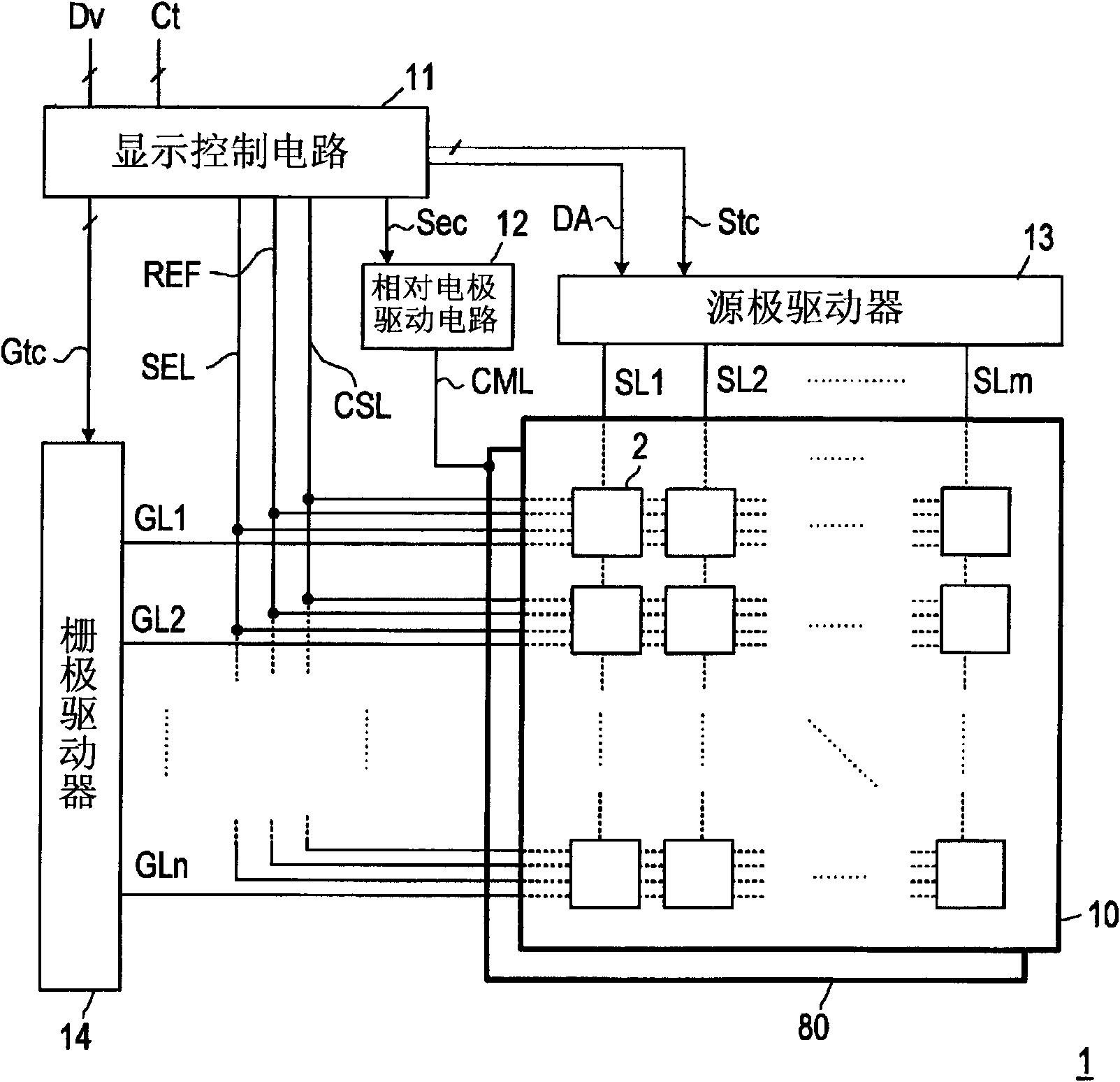
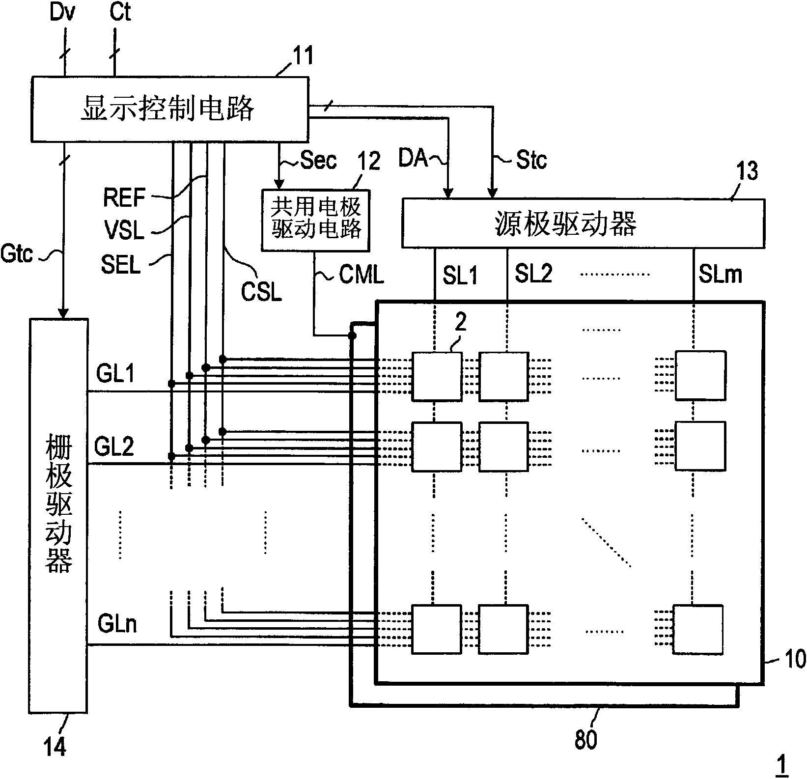
[0113] In the first embodiment, circuit configurations of a display device of the present invention (hereinafter referred to as a display device) and a pixel circuit of the present invention (hereinafter referred to as a pixel circuit) will be described.
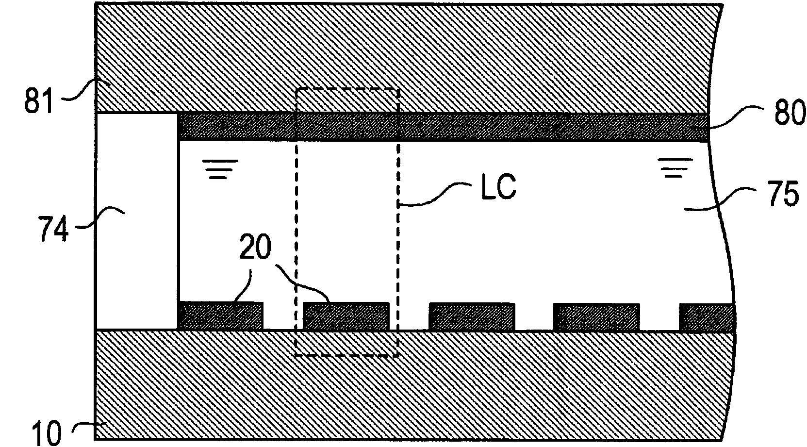
[0114] figure 1 A schematic configuration of the display device 1 is shown. The display device 1 includes an active matrix substrate 10 , counter electrodes 80 , a display control circuit 11 , a counter electrode drive circuit 12 , a source driver 13 , a gate driver 14 , and various signal lines described later. On the active matrix substrate 10, a plurality of pixel circuits 2 are respectively arranged in the row direction and the column direction to form a pixel circuit array. In addition, in figure 1 In , the pixel circuit 2 is displayed in blocks in order to avoid the complexity of the drawings. In addition, in figure 1 In , in order to clearly show that various signal lines are formed on the active matrix substra...
no. 2 Embodiment approach
[0146] In the second embodiment, description will be made by type with reference to drawings Figure 5 ~ Figure 8 , Figure 11 and Figure 12 The illustrated self-polarity inversion operation of the pixel circuits 2A to 2F constituted by circuits of the first type to the sixth type is shown. In addition, the self-polarity inversion operation refers to an operation in which the first switch circuit 22, the second switch circuit 23, and the control circuit 24 are operated in a predetermined order for a plurality of pixel circuits 2 by the operation in the constant display mode. The polarity of the liquid crystal voltage Vlc applied between the pixel electrode 20 and the counter electrode 80 is also reversed while maintaining its absolute value. Therefore, all gate lines GL, source lines SL, selection lines SEL, reference lines REF, storage capacitor lines CSL, voltage supply lines VSL, and counter electrodes connected to the pixel circuit 2 to be subjected to the self-polarity...
no. 3 Embodiment approach
[0197] In the third embodiment, description will be made by type with reference to the drawings Figure 5 ~ Figure 8 , Figure 11 and Figure 12 The write operation in the constant display mode is performed by the pixel circuits 2A to 2F of circuit configurations of the illustrated first to sixth types.
[0198] The writing operation in the constant display mode is an operation in which the pixel data for one frame is divided into each display line in the horizontal direction (row direction), and the source lines SL of each column are written in each horizontal period. A binary voltage (high level (5V) or low level (0V)) corresponding to each pixel data of one display line is applied, and selection is applied to the gate line GL of the selected display line (selection row). A row voltage of 8V turns on the first switch circuits 22 of all the pixel circuits 2 in the selected row, and transfers the voltage of the source line SL of each column to the internal node N1 of each pi...
PUM
 Abstract
Description
Claims
Application Information
 - R&D
- Intellectual Property
- Life Sciences
- Materials
- Tech Scout
- Unparalleled Data Quality
- Higher Quality Content
- 60% Fewer Hallucinations
Browse by: Latest US Patents, China's latest patents, Technical Efficacy Thesaurus, Application Domain, Technology Topic, Popular Technical Reports.
© 2025 PatSnap. All rights reserved.Legal|Privacy policy|Modern Slavery Act Transparency Statement|Sitemap|About US| Contact US: help@patsnap.com