Methanol gas sensor based on organic filter transistor and preparation method of methanol gas sensor
A formaldehyde gas and organic thin film technology, applied in the direction of instruments, scientific instruments, measuring devices, etc., can solve the problems of harsh preparation environment, high preparation cost, low sensitivity, etc., and achieve suitable for large-scale industrial production, large response current, low cost effect
- Summary
- Abstract
- Description
- Claims
- Application Information
AI Technical Summary
Problems solved by technology
Method used
Image
Examples
Embodiment 1
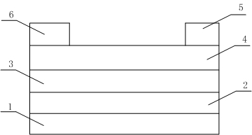
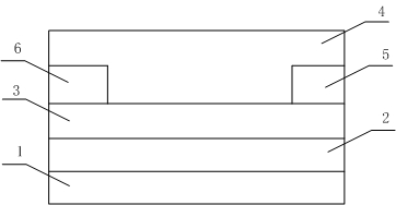
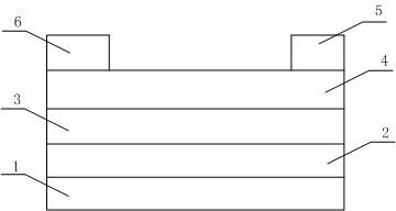
[0038] Device structure such as figure 1 As shown, it is a bottom-gate top-contact structure. The material and thickness of each layer of the device are as follows: the substrate 1 is glass, the gate electrode 2 is ITO with a thickness of 180 nm, the gate insulating layer 3 is PMMA with a thickness of 500 nm, and the formaldehyde gas organic semiconductor detection layer 4 is pentacene , the thickness is 25nm, the source electrode 5 and the drain electrode 6 are both Au, the thickness is 50nm.
[0039] Its preparation method is as follows:
[0040] ① Thoroughly clean the glass substrate 1 on which the gate electrode ITO has been sputtered, and dry it with dry nitrogen after cleaning;
[0041] ② Preparing PMMA film on ITO by spin coating method to form gate insulating layer 3;
[0042] ③Heating and baking the spin-coated PMMA film;
[0043] ④ Vacuum evaporation is used to prepare the pentacene gas organic semiconductor detection layer 4;
[0044] ⑤ Prepare the source elect...
Embodiment 2
[0046] The structure of the sensor is as figure 1 shown. The material and thickness of each layer of the sensor are: substrate 1 is glass, gate electrode 2 is ITO with a thickness of 180 nm, gate insulating layer 3 is PS with a thickness of 20 nm, formaldehyde gas organic semiconductor detection layer 4 is pentacene , with a thickness of 25 nm, and the source electrode 5 and the drain electrode 6 are both Au with a thickness of 50 nm.
[0047] The preparation process is similar to Example 1.
Embodiment 3
[0049] The sensor structure is as figure 1 shown. The material and thickness of each layer of the sensor are as follows: the substrate 1 is glass, the gate electrode 2 is ITO with a thickness of 180 nm, the gate insulating layer 3 is PVA with a thickness of 2000 nm, and the formaldehyde gas organic semiconductor detection layer 4 is pentacene , the thickness is 25nm, the source electrode 5 and the drain electrode 6 are both Au, the thickness is 50nm.
[0050] The preparation process is similar to Example 1.
PUM
| Property | Measurement | Unit |
|---|---|---|
| thickness | aaaaa | aaaaa |
| thickness | aaaaa | aaaaa |
| thickness | aaaaa | aaaaa |
Abstract
Description
Claims
Application Information


