Method for quickly and nondestructively measuring thickness and band structure of graphene film

A technology of graphene film and energy band structure, which is applied in the direction of measuring devices, instruments, and polarization-influenced characteristics, to achieve the effects of increasing detection speed, reducing difficulty, and simplifying complexity

Inactive Publication Date: 2012-06-20
FUDAN UNIV
View PDF3 Cites 12 Cited by
  • Summary
  • Abstract
  • Description
  • Claims
  • Application Information

AI Technical Summary

Problems solved by technology

[0004] The purpose of the present invention is to propose a method for fast and non-destructive measurement of graphene film thickness and energy band structure that is adapta

Method used


Image

  • Method for quickly and nondestructively measuring thickness and band structure of graphene film
  • Method for quickly and nondestructively measuring thickness and band structure of graphene film
  • Method for quickly and nondestructively measuring thickness and band structure of graphene film

Examples


Embodiment Construction

[0017] The present invention will be further described in detail below in conjunction with the accompanying drawings and specific embodiments. The method for measuring the energy gap gradient of graphene thin films proposed by the present invention can be applied to the measurement of electronic energy gaps of graphene thin films such as FRGO and GO. What is described below takes the detection of energy gap changes before and after the reduction of GO thin films as an example. process flow.

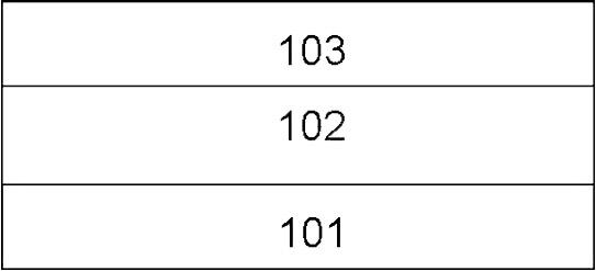
[0018] First, grow a layer of SiO on the silicon substrate 101 2 Thin film 102, then transfer GO or FRGO to SiO 2 On, generate thin film 103, such as figure 1 shown.

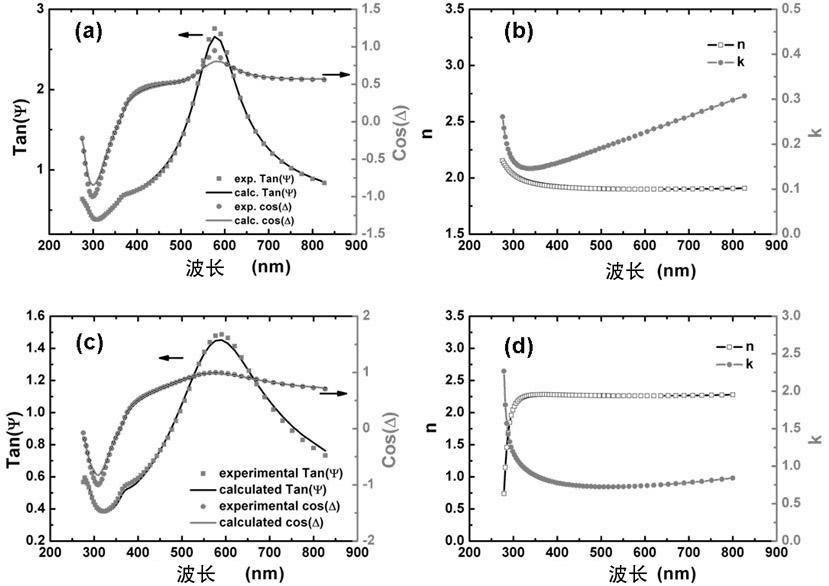
[0019] Next, the ellipsometric data of GO and FRGO thin films were obtained by ellipsometry, and the spectra of GO and FRGO thin films are as follows figure 2 (a) and (c) are shown by the solid line.

[0020] Next, establish a theoretical model, here we use the classic Lorentz oscillator model for analysis. The compl...


PUM


Abstract

The invention belongs to the technical field of integrated semiconductor circuit fabrication, and provides a method for quickly and nondestructively measuring thickness and energy gap of a graphene film. The method of the invention comprises the steps of: firstly obtaining elliptical polarization data of the film by elliptical polarization technology; and then, creating a proper theoretical model according to the structure of the measured film to analyze and fit the obtained elliptical polarization data so as to obtain the thickness and band structure of the measured graphene film. The method of the invention has the advantages of greatly simplifying the thickness test complexity of the ultrathin films and reducing the construction difficulty of other techniques, so that the method has an important application value in fabrication of large scale integrated circuits larger than 22 nanometers.

Description

technical field [0001] The invention relates to a method for measuring the thickness and energy band structure of a graphene film, in particular to a method for rapidly and non-destructively measuring the energy band structure of a graphene film applied in the manufacture of large-scale integrated circuits after 22 nanometers, belonging to the manufacture of semiconductor integrated circuits technology field. Background technique [0002] With the continuous development of semiconductor technology, the continuous extension and depth of Moore's Law has made the size of silicon-based integrated circuit devices closer and closer to its physical limit. The international semiconductor development roadmap ITRS has planned the MOSFET materials and processes in the 16nm feature size technology, among which the most important thing in the MOSFET is the selection and control of the gate oxide layer, such as TiO 2 , aluminum-doped titanium oxide, hafnium oxide, zirconium oxide, etc. H...

Claims


Application Information

Patent Timeline
IPC IPC(8): G01N33/00G01N21/21
Inventor 周鹏沈彦孙清清王鹏飞张卫
Owner FUDAN UNIV
Why Eureka
Try Eureka