

Monitoring semiconductor substrate test structures and test methods for integrated passive devices
A technology for integrating passive devices and test structures, applied in semiconductor devices, semiconductor/solid-state device parts, electric solid-state devices, etc., can solve problems such as reducing inductance and Q coefficient, small resistivity, high-frequency signal loss, etc.
- Summary
- Abstract
- Description
- Claims
- Application Information
AI Technical Summary
Problems solved by technology
Method used
Image

Examples
Embodiment Construction
[0019] In order to make the content of the present invention clearer and easier to understand, the content of the present invention will be described in detail below in conjunction with specific embodiments and accompanying drawings.
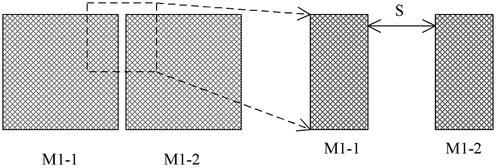
[0020] figure 1 A test structure for monitoring a semiconductor substrate for integrating passive devices according to an embodiment of the present invention is schematically shown. Among them, passive components are used in high frequency applications.
[0021] in, figure 1 The middle right view shows a partial enlargement of the left view.
[0022] like figure 1 As shown, which shows a partial layout structure of the top metal layer, where M1-1 and M1-2 represent two metal lines in the top metal layer (first metal layer) of the semiconductor integrated circuit, and the first metal line M1- 1 and the second metal line M1-2. The areas of the first metal line M1 - 1 and the second metal line M1 - 2 are not specifically limited, for example, ...
PUM
 Abstract
Description
Claims
Application Information