Layout bipartition method

A two-partition and layout technology, applied in special data processing applications, instruments, electrical digital data processing, etc., can solve the problems of high density, affecting the quality of chip manufacturing, and the production cost has no good prospects, etc., to achieve high accuracy and partition Reasonable results and convenient follow-up adjustments

Active Publication Date: 2012-06-27
TSINGHUA UNIV
View PDF2 Cites 22 Cited by
  • Summary
  • Abstract
  • Description
  • Claims
  • Application Information

AI Technical Summary

Problems solved by technology

For the 32nm / 22nm layout, due to the small size and high density of the pattern, the pattern on the photoresist will be deformed under the existing photolithography technology, which will seriously affect the quality of chip manufacturing
The new photolithography technology, including extreme ultraviolet technology and immersion argon fluoride technology, has no good prospects in terms of process and production cost.

Method used


Image

  • Layout bipartition method
  • Layout bipartition method
  • Layout bipartition method

Examples


Embodiment Construction

[0047] The present invention will be described in detail below in conjunction with the accompanying drawings and embodiments.

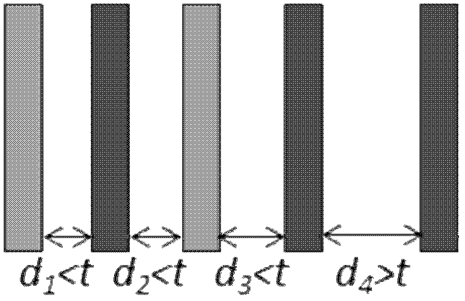
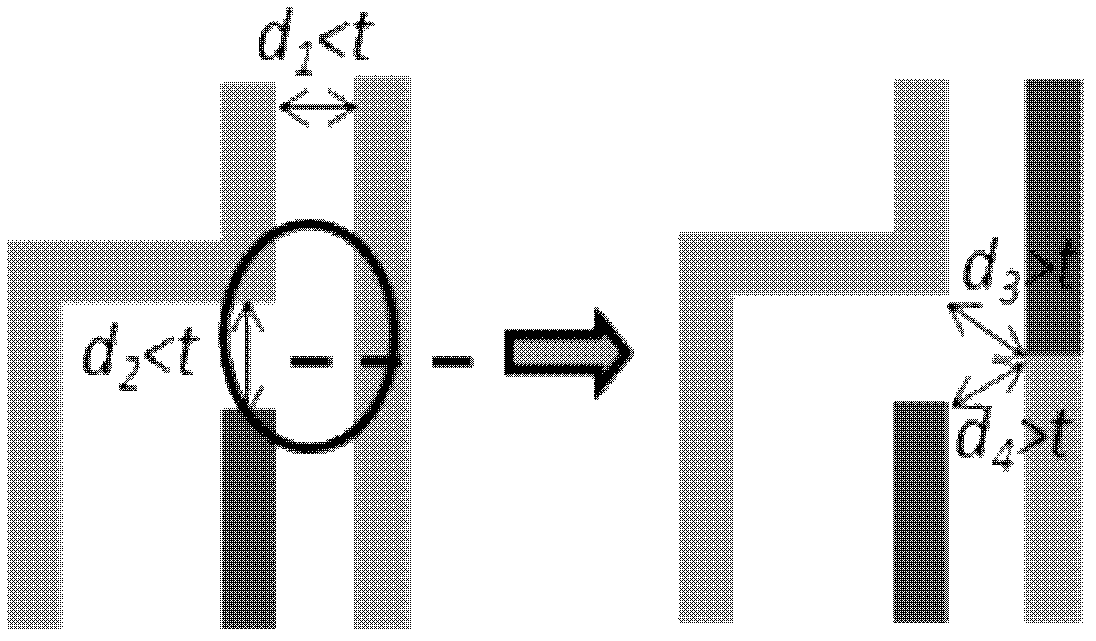
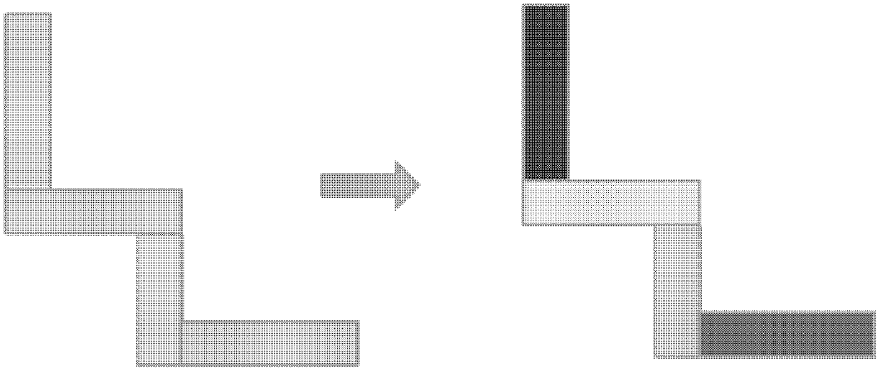
[0048] The double layout lithography technology is a method to solve the defect that the product quality is reduced due to the excessive layout density in the lithography process. The double layout lithography technology refers to dividing the content on a mask with high density into two masks at intervals on the basis of the existing lithography technology, so that the transistors on the two masks The density meets the standard of the existing photolithography technology, and then undergoes two photolithography etchings to restore the original mask. The principle is as Figure 1 to Figure 3 shown.

[0049] The invention proposes a method for bipartitioning the layout of an integrated circuit, by using the method, the layout of an integrated circuit can be reasonably divided into two according to the requirements of the double layout photolithograph...


PUM


Abstract

The invention discloses a layout bipartition method, aiming at solving the defect that the product quality is lowered due to overlarge layout density in the conventional photoetching technology. The layout bipartition method disclosed by the invention comprises the following steps of: partitioning graphs of which the graph pitch is less than a minimal photoetching pitch, into two sub layouts, and obtaining a layout graph through two photoetching operations; when the graph pitch in the sub layout is still less than the minimal photoetching pitch after two sub layouts are formed, partitioning the graphs in the layouts into at least two sub graphs, partitioning each sub graph of which the pitch is less than the minimal photoetching pitch, into two sub layouts by using the sub graph as a unit, and obtaining the layout graph after carrying out two photoetching operations on a substrate; and labeling the layout region where sub layouts cannot be obtained by using a partitioning method. The layout bipartition method disclosed by the invention is applied to the fields of layout design and product manufacture of large-scale integration circuits, and has the characteristics of convenience for use and high accuracy.

Description

technical field [0001] The present invention relates to a version Figure II division method. Background technique [0002] In the mainstream microelectronics manufacturing process, photolithography is an indispensable process, and it is also the most complex, expensive and critical process. In the manufacturing process of integrated circuits, dozens of photolithography processes are often required. At present, the mainstream technology of integrated circuit manufacturing process is photolithography technology using ultraviolet light including far ultraviolet light as light source. With the development of chips in the direction of smaller size and higher density, lithography technology has also encountered new challenges. For the 32nm / 22nm layout, due to the small size and high density of the pattern, the pattern on the photoresist will be deformed under the existing photolithography technology, which will seriously affect the quality of chip manufacturing. The new photol...

Claims


Application Information

Patent Timeline
Patent Type & Authority Applications(China)
IPC IPC(8): G06F17/50
Inventor 蔡懿慈姚海龙邓超
Owner TSINGHUA UNIV
Why Eureka
Try Eureka