Reading and writing optimization method of embedded memory

A technology of embedded memory and optimization method, applied in the direction of memory address/allocation/relocation, etc., can solve the problems of eflash cannot be read and written by word, long time, large page size, etc., to achieve simple and efficient read and write operations, and improve performance , the effect of reducing complexity

Active Publication Date: 2012-07-04
SHANGHAI AISINOCHIP ELECTRONICS TECH
View PDF3 Cites 9 Cited by
  • Summary
  • Abstract
  • Description
  • Claims
  • Application Information

AI Technical Summary

Problems solved by technology

[0004] However, eflash has disadvantages in application: on the one hand, eflash cannot read and write by word; on the other hand, eflash can only perform erasing operations in page units, and a page is usually very large, ranging from 256 bytes to 4K bytes are available
In addition, before writing to eflash, an erase operation must be performed, and the erase operation takes a very long time, generally reaching the microsecond level
This will bring a lot of inconvenience in the application, increase the complexity of the file system implementation, and reduce the system performance

Method used


Image

  • Reading and writing optimization method of embedded memory
  • Reading and writing optimization method of embedded memory
  • Reading and writing optimization method of embedded memory

Examples


Embodiment Construction

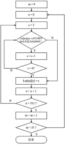
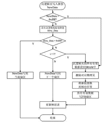
[0025] The present invention is a reading and writing optimization method suitable for embedded Norflash memory (hereinafter referred to as eflash). First, each physical page of eflash is divided into several physical sectors of the same size, which are usually divided into 4 or 8 sectors for easy counting. physical sectors. Make a physical page correspond to a logical page, and at the same time, make a logical page correspond to several physical sectors of the same size, that is, the data on the same logical page will be distributed on different sectors of the same physical page, and a logical page The size is equal to the size of a physical sector.

[0026] The application program specifically accesses the data on the logical page, and the data on the logical page needs to go through a specific mapping relationship to correspond to the data on the real physical page. For this reason, a kind of efficient mapping relationship is defined in the present invention, namely, make ...


PUM


Abstract

The invention relates to a reading and writing optimization method of an embedded memory, which is applicable to an eflash memory. The reading and writing optimization method comprises the following steps of: enabling a plurality of sectors with the same sizes on a logical page to correspond to a plurality of sectors with the same sizes on a physical page, and establishing a mapping relation between effective data on the logical page and the sectors on the physical page. Actually-stored data is found out for reading according to the mapping relation. In the writing operation, the actually-stored data is firstly read, if the data is a FF (Full Figure), the data is directly written; if the data is not the full figure, and the current sector is not positioned in the last sector, the data is written into the next sector, otherwise, all effective data on the current logical page is read into an SRAM (Static Random Access Memory), the corresponding physical page is erased, and values in the SRAM are written into the first sector on the erased physical page after being updated into latest values; and after the operation is finished, a mapping table is updated. The optimization method has the beneficial effects that the reading and writing operation of the eflash memory is simplified, the performance of a file system can be effectively improved, and the complexity of the system is simultaneously reduced.

Description

technical field [0001] The invention relates to a method for optimizing reading and writing of an embedded Norflash memory (hereinafter referred to as eflash), and is especially suitable for an embedded software system that establishes a file system on the eflash. Background technique [0002] Semiconductor memory can be divided into two types: volatile memory and non-volatile memory. Volatile memory loses the stored data after power failure, while non-volatile memory can protect data even when the power is cut off. ROM is a non-volatile memory. ROM is divided into two types according to whether the user can write data. One is the ROM that the user can write, and the other is the ROM written by the manufacturer during the processing process. Mask ROM. Among the ROMs that can be written by users, EEPROM (Electrically Erasable Programmable ROM) and eflash (Embedded Flash Memory) are commonly used. [0003] eflash is the product of the maturity of EEPROM, the development of s...

Claims


Application Information

Patent Timeline
Patent Type & Authority Applications(China)
IPC IPC(8): G06F12/06
Inventor 陈诚朱念好周玉洁
Owner SHANGHAI AISINOCHIP ELECTRONICS TECH
Why Eureka
Try Eureka