Method for manufacturing transparent silicon-based substrate with integrated circuit (IC) device

A manufacturing method and device technology, applied in semiconductor/solid-state device manufacturing, electrical components, circuits, etc., can solve the problems of large module volume, complex optical path structure, and reduced light utilization rate of the optical path, and achieve simple structure, simple optical path, and compact effect

Active Publication Date: 2012-07-04
NANJING GUOZHAO OPTOELECTRONICS TECH CO LTD
View PDF2 Cites 5 Cited by
  • Summary
  • Abstract
  • Description
  • Claims
  • Application Information

AI Technical Summary

Problems solved by technology

[0005] The purpose of the present invention is to solve the problem that the existing opaque silicon-based substrate requires PBS optical devices to realize normal display, which causes the light utilization rate of the entire optical path to be reduced, the optical path structure is complex, and the entire module is large in size, which does not meet the requirements of helmets or near-eye displays, etc. The field requires micro-display devices to be small in size and light in weight, and to invent a method for manufacturing a transparent silicon-based substrate with IC devices that can realize imaging without PBS optical devices

Method used


Image

  • Method for manufacturing transparent silicon-based substrate with integrated circuit (IC) device
  • Method for manufacturing transparent silicon-based substrate with integrated circuit (IC) device
  • Method for manufacturing transparent silicon-based substrate with integrated circuit (IC) device

Examples


Embodiment Construction

[0037] The present invention will be further described below in conjunction with the accompanying drawings and embodiments.

[0038] Such as Figure 1-8 shown.

[0039] A method for manufacturing a transparent silicon-based substrate with an IC device, comprising the following steps:

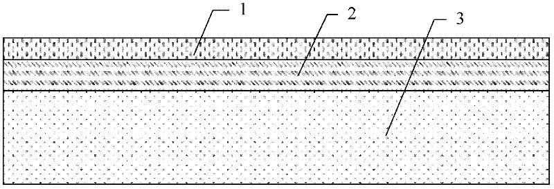
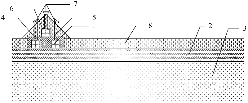
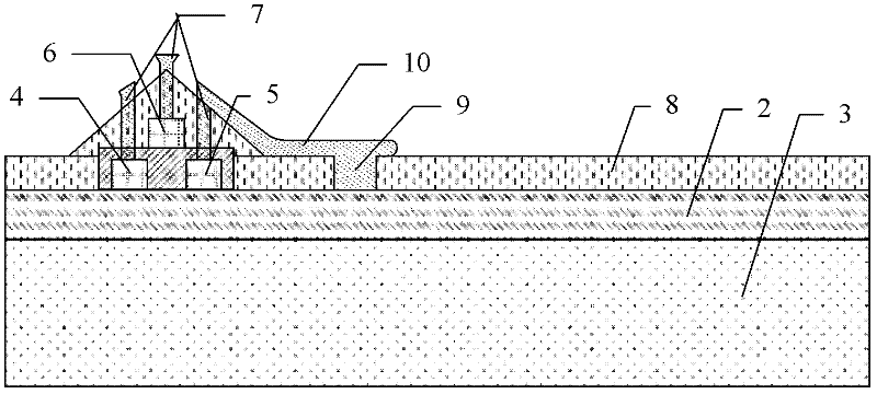
[0040] 1) Select a silicon-on-insulator (SOI, SILICON ON INSULATOR) as the substrate for making IC devices. The silicon-insulator is composed of a substrate silicon layer 3, a silicon dioxide insulating layer 2, and a device silicon layer 1. The device silicon layer 1 Located on the top layer, the silicon dioxide insulating layer 2 is located between the substrate silicon layer 3 and the device silicon layer 1;

[0041] To make transparent silicon-based substrates, general bulk silicon cannot meet the requirements, and special silicon wafers are required. This invention uses SOI (SILICON ON INSULATOR) insulating silicon wafers, which are devices made of substrate silicon, silicon dioxide insul...


PUM


Abstract

The invention discloses a method for manufacturing a transparent silicon-based substrate with an integrated circuit (IC) device. The method comprises the following steps of: manufacturing an IC-on-silicon part on a silicon-on-insulator; adhering the silicon-on-insulator and a transparent substrate by using optical glue; removing a silicon base by using a mechanical thinning and chemical etching method, so that a silicon-based substrate is transparent; and punching a silicon dioxide layer, leading out an electrode and patterning. A device made of the transparent silicon-based substrate has the advantages of simple structure, high reliability, high aperture ratio and the like.

Description

technical field [0001] The invention relates to a method for manufacturing a substrate for a transmissive silicon-based thin film transistor, in particular to a method for manufacturing a transmissive silicon-based transparent substrate used in the fields of microdisplay, photodetection, optical communication, consumer electronics, etc. . Specifically, it is a manufacturing method of a transparent silicon-based substrate with IC devices. Background technique [0002] At present, the general silicon-based substrate is opaque, and its reflective use is mainly used in the display field. For example, LCOS (Liquid Crystal on Silicon) is a reflective liquid crystal device with high integration, high resolution, The device itself has the characteristics of high aperture ratio, and is widely used in the field of microdisplay. However, in the optical system of reflective liquid crystal on silicon, it is necessary to add an additional polarization beam splitter PBS device, which is ...

Claims


Application Information

Patent Timeline
Patent Type & Authority Applications(China)
IPC IPC(8): H01L21/762
Inventor 杨洪宝余雷洪乙又樊卫华铁斌王绪丰
Owner NANJING GUOZHAO OPTOELECTRONICS TECH CO LTD
Why Eureka
Try Eureka