

MOS (metal oxide semiconductor) power device and manufacturing method thereof
A technology of power devices and manufacturing methods, applied in the direction of semiconductor/solid-state device manufacturing, semiconductor devices, electrical components, etc.
- Summary
- Abstract
- Description
- Claims
- Application Information
AI Technical Summary
Problems solved by technology
Method used
Image

Examples
Embodiment Construction
[0036] In order to make the technical problems, technical solutions and beneficial effects solved by the present invention clearer, the present invention will be further described in detail below in conjunction with the accompanying drawings and embodiments. It should be understood that the specific embodiments described here are only used to explain the present invention, not to limit the present invention.
[0037] Figures 3a to 3h A flow chart of a manufacturing method for a MOS type power device provided by an embodiment of the present invention; as Figures 3a to 3h The manufacturing method of a kind of MOS type power device shown, comprises the following steps:
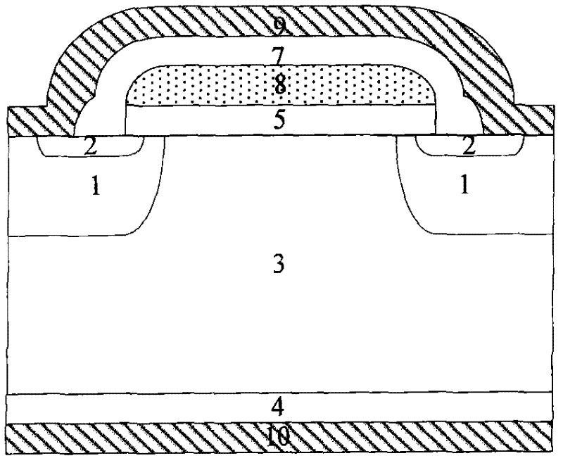
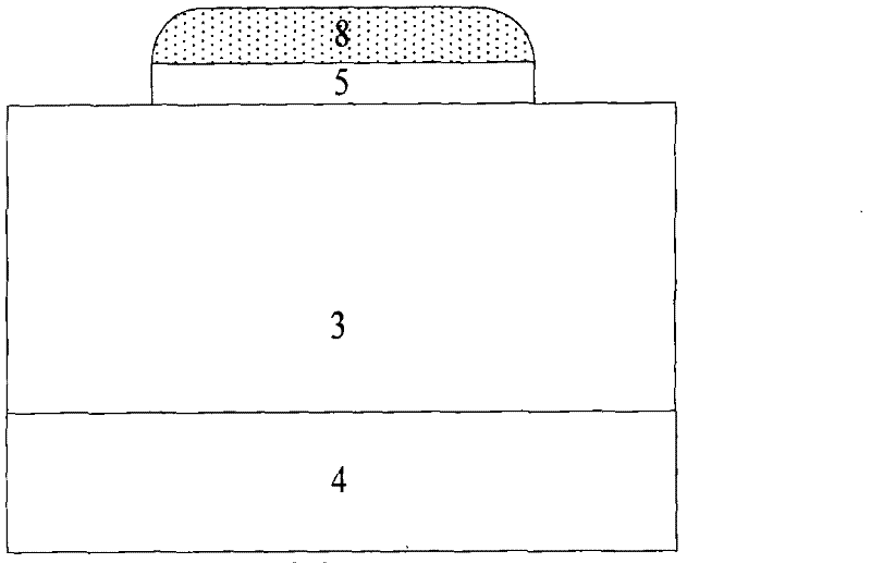
[0038] (1) if Figure 3a As shown: a first oxide layer 5 is formed on a semiconductor substrate 3; in this embodiment, the first oxide layer is specifically a gate oxide layer with a thickness of 0.02um to 0.12um, and is specifically formed on the on the semiconductor substrate.
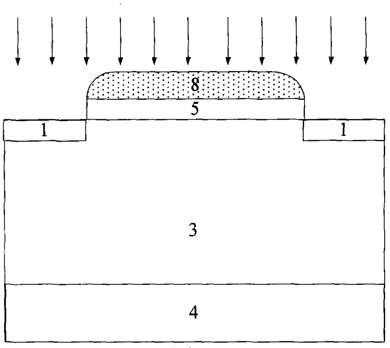
[0039] (2) if Figure 3b ...
PUM
 Abstract
Description
Claims
Application Information