
A segmented type asymmetric silicon controlled rectifier electrostatic discharge device embedded with P+ injection regions

A technology of electrostatic discharge and injection area, applied in the direction of electric solid devices, electrical components, semiconductor devices, etc., can solve the problems of high device sustaining voltage, failure current drop, etc., achieve high sustaining voltage, increase sustaining voltage, and increase parasitic resistance. Effect

Active Publication Date: 2020-02-21
XIANGTAN UNIV
View PDF4 Cites 3 Cited by
  • Summary
  • Abstract
  • Description
  • Claims
  • Application Information

AI Technical Summary

Problems solved by technology

Often the higher the maintenance voltage of the device, the failure current will drop

Method used


Image

  • A segmented type asymmetric silicon controlled rectifier electrostatic discharge device embedded with P+ injection regions
  • A segmented type asymmetric silicon controlled rectifier electrostatic discharge device embedded with P+ injection regions
  • A segmented type asymmetric silicon controlled rectifier electrostatic discharge device embedded with P+ injection regions

Examples


Embodiment Construction

[0033] The present invention will be further described below in conjunction with the accompanying drawings and embodiments.

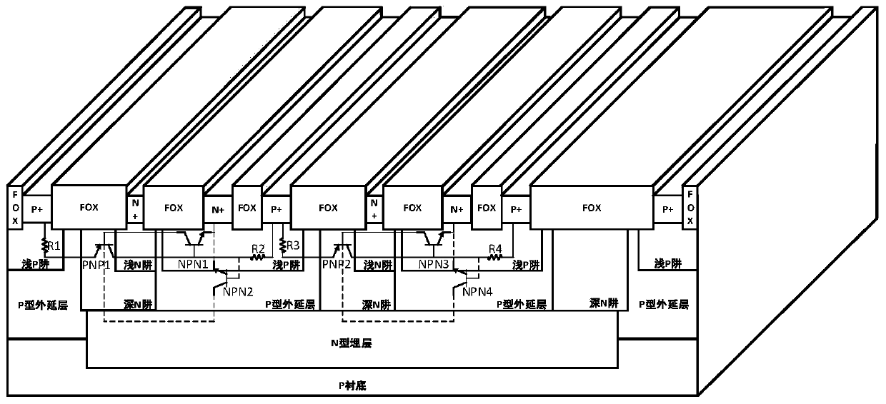
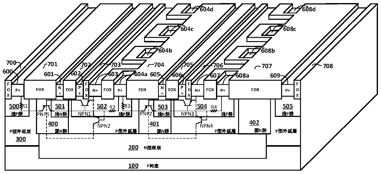
[0034] Such as image 3 As shown, a segmented asymmetric thyristor electrostatic discharge device embedded in a P+ implantation area includes a P-type substrate 100; a P-type epitaxial layer 300 is arranged above the P-type substrate 100, and the P-type substrate 100 and An N-type buried layer 200 is disposed between the P-type epitaxial layers 300 ; a first deep N well 400 , a second deep N well 401 and a third deep N well 402 are sequentially disposed above the N-type buried layer from left to right.

[0035] The left side of the first deep N well 400 is provided with a first shallow P well 500, and the upper right of the first deep N well 400 is provided with a first shallow N well 501, between the first deep N well 400 and the second deep N well 401 A second shallow P well 502 is arranged between them, a second shallow N well 503 is arranged in the...


PUM


Abstract

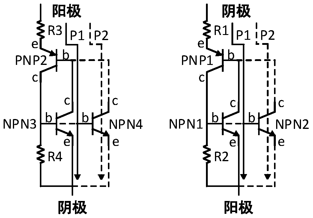
The invention discloses a segmented type asymmetric silicon controlled rectifier electrostatic discharge device embedded with P+ injection regions. The device is characterized in that, to begin with,a floating P+ injection region is added into a shallow P well, so that the width and concentration of a base electrode of a transverse parasitic NPN transistor are increased, the amplification times of the transverse parasitic NPN transistor is reduced, static electricity tends to be discharged from a longitudinal parasitic NPN transistor, a current path becomes deeper and longer, and the maintaining voltage of the device can be effectively improved; then, the P+ injection region used for ohmic contact of the shallow P well adopts a segmented structure, so that the parasitic resistance of theshallow P well is increased; and meanwhile, an N+injection region adopts a comb-shaped structure, so that the emitter area of a parasitic triode can be increased, the emission efficiency can be improved, and the failure current of the device can be effectively improved. The silicon controlled rectifier electrostatic discharge device has the characteristics of high maintaining voltage and high failure current, and can realize a high protection level while effectively avoiding a latch-up effect.

Description

technical field [0001] The invention relates to the field of electrostatic protection, in particular to a segmented asymmetric thyristor electrostatic discharge device embedded in a P+ injection area. Background technique [0002] Electro-Static Discharge (ESD) is an inevitable phenomenon in the process of manufacturing, packaging, testing, transportation, assembly and use of integrated circuits. There are internal and external reasons for the generation of static discharge points. Static electricity accounts for 58% of the various reasons for the failure of integrated circuits, which poses a serious threat to the reliability of integrated circuits. There are two ways to protect integrated circuits from static electricity: one is to control and reduce the occurrence of static electricity and discharge, such as using electrostatic protective clothing, anti-static wrist straps, etc.; the other is to design static discharge devices around the chip to provide static discharge. ...

Claims


Application Information

Patent Timeline
Patent Type & Authority Applications(China)
IPC IPC(8): H01L27/02H01L29/06
CPCH01L27/0207H01L27/0248H01L29/0684
Inventor 汪洋陈锡均夹丹丹芦俊杨红姣周子杰
Owner XIANGTAN UNIV
Learn More