Power MOS field effect transistor integrated with depletion startup device

A field-effect transistor, depletion-mode technology, applied in the field of semiconductor power devices, can solve the problems of reducing the economic benefits of AC-DC switching power supply manufacturers, increasing the production cost of AC-DC switching power supplies, and complex high-voltage integration processes, and achieving simplification. The effect of semiconductor manufacturing process, simplifying circuit design complexity, and reducing layout area

Active Publication Date: 2016-02-03
SUZHOU KAIWEITE SEMICON
View PDF5 Cites 3 Cited by
  • Summary
  • Abstract
  • Description
  • Claims
  • Application Information

AI Technical Summary

Problems solved by technology

However, the high-voltage integration process adopted by this method is relatively complicated and costly, which indirectly increases the production cost of AC-DC switching power supply and reduces the economic benefits of AC-DC switching power supply manufacturers.

Method used


Image

  • Power MOS field effect transistor integrated with depletion startup device
  • Power MOS field effect transistor integrated with depletion startup device
  • Power MOS field effect transistor integrated with depletion startup device

Examples


Embodiment Construction

[0019] In order to deepen the understanding and knowledge of the present invention, the present invention will be further described and introduced in conjunction with the accompanying drawings.

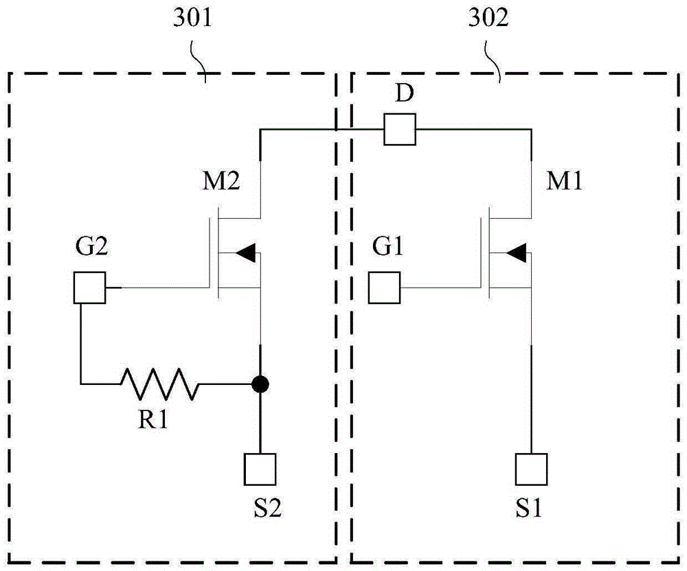
[0020] Such as image 3 As shown, a power MOS field effect tube integrated with a depletion type start device includes an enhancement mode MOS field effect tube M1, a depletion mode MOS field effect tube M2 and a POLY resistor R1. The enhancement mode MOS field effect tube M1 and The depletion type MOS field effect transistor M2 has a common drain connection. A POLY resistor R1 is connected in series between the gate and the source of the depletion type MOS field effect transistor M2. The enhanced MOS field effect transistor M1 and the depletion type MOS The common drain of the field effect tube M2 is led out as the drain electrode D of the power MOS field effect tube, and the gate of the enhancement mode MOS field effect tube M1 is led out as the first gate electrode G1 of the power MOS ...


PUM


Abstract

The invention relates to a power MOS field effect transistor integrated with a depletion startup device. The power MOS field effect transistor comprises an enhanced MOS field effect transistor, a depletion MOS field effect transistor and a POLY resistor, wherein the enhanced MOS field effect transistor and the depletion MOS field effect transistor are connected in a common drain; the POLY resistor is connected between a grid and a source of the depletion MOS field effect transistor in series; the common drain of the enhanced MOS field effect transistor and the depletion MOS field effect transistor is led out as a drain electrode of the power MOS field effect transistor; the grid of the enhanced MOS field effect transistor is led out as a first gate electrode of the power MOS field effect transistor; the source of the enhanced MOS field effect transistor is led out as a first source electrode of the power MOS field effect transistor; a connection end of the source of the depletion MOS field effect transistor and the POLY resistor is led out as a second source electrode of the power MOS field effect transistor; and the connection end of the grid of the depletion MOS field effect transistor and the POLY resistor is led out as a second gate electrode of the power MOS field effect transistor. The overall power MOS field effect transistor is low in power consumption; the design complexity is simplified; and the cost is reduced.

Description

Technical field [0001] The invention relates to a semiconductor power device, in particular to a power MOS field effect tube, in particular to a power MOS field effect tube integrating a depletion type start device. Background technique [0002] The block diagram of the traditional AC-DC switching power supply is attached figure 1 As shown, the startup circuit 101 and the PWM circuit 102 in the AC-DC switching power supply are integrated to form the control circuit of the power supply, and the power switch tube M1 is used as the output stage connection switch SW. When the circuit works, the control circuit outputs a driving signal to control the switching of the power switch tube M1. In most cases, the startup resistor R1 is used to supply power to the startup circuit 101 between the startup circuit 101 in the control circuit on the power supply and the AC power supply ACIN. However, because the startup resistor R1 is in the process of system standby, there is always energy consu...

Claims


Application Information

Patent Timeline
Patent Type & Authority Applications(China)
IPC IPC(8): H01L27/085
Inventor 丁国华罗寅谭在超张海滨
Owner SUZHOU KAIWEITE SEMICON
Why Eureka
Try Eureka