Substrate heating chamber, method using same, and substrate processing equipment

A substrate processing equipment and substrate processing technology, applied in the direction of ion implantation plating, metal material coating process, coating, etc., can solve the problems that the capacity of the magnetron sputtering system cannot be fully utilized and the time is long, and achieve Make full use of capacity, meet capacity demand, and avoid the effect of idle state

Active Publication Date: 2012-07-11
BEIJING NAURA MICROELECTRONICS EQUIP CO LTD
View PDF9 Cites 10 Cited by
  • Summary
  • Abstract
  • Description
  • Claims
  • Application Information

AI Technical Summary

Problems solved by technology

Since the degassing process is the first step of the entire sputtering process and this process takes the longest time, and because each degassing chamber can only process one substrate at a time; H

Method used


Image

  • Substrate heating chamber, method using same, and substrate processing equipment
  • Substrate heating chamber, method using same, and substrate processing equipment
  • Substrate heating chamber, method using same, and substrate processing equipment

Examples


Embodiment Construction

[0029] In order for those skilled in the art to better understand the technical solution of the present invention, the substrate heating chamber, the method for using the substrate heating chamber and the substrate processing equipment provided by the present invention will be described in detail below with reference to the accompanying drawings.

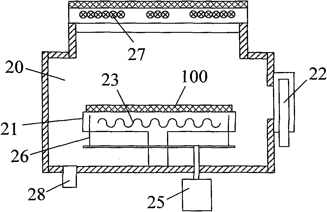
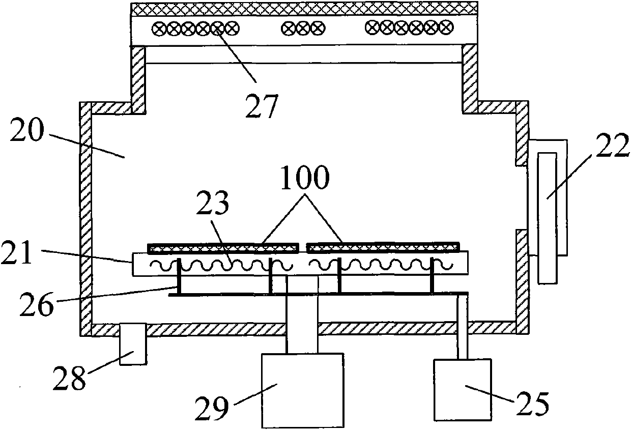
[0030] The substrate heating chamber provided by the present invention can simultaneously heat at least two substrates, and is used for heating the substrates before the substrate processing process. With the help of the substrate heating chamber provided by the present invention, the efficiency of the substrate heating process can be effectively improved to meet the production capacity requirements of the substrate processing process, and avoid the problem that the substrate processing process chamber is often in an idle state due to waiting for the substrate to be heated. Thus, the production capacity of the substrate processing eq...


PUM


Abstract

The invention provides a substrate heating chamber, a method using the substrate heating chamber, and substrate processing equipment. The substrate heating chamber can be used for heating up at least two of substrates simultaneously, and is used for heating up the substrate before a substrate processing technology. The substrate is heated by the substrate heating chamber, so that the problem that the follow-up substrate processing technology is under the idle condition since the substrate is waited to be heated up can be effectively avoided; and therefore, the capacity factor of the equipment can be effectively improved. Furthermore, according to the method using the substrate heating chamber and the substrate processing equipment, the capacity factor of the equipment can be effectively improved.

Description

technical field [0001] The invention relates to the technical field of microelectronic processing, in particular to a substrate heating chamber, a method for using the substrate heating chamber and substrate processing equipment. Background technique [0002] With the continuous advancement of integrated circuit production technology, the integration level of circuit chips has been greatly improved. At present, the number of transistors integrated in a chip has reached an astonishing tens of millions, and the signal integration of such a large number of active components requires more than ten layers of high-density metal interconnection layers for connection. Therefore, as an important process for preparing the above-mentioned metal interconnection layer, physical vapor deposition (Physical Vapor Deposition, hereinafter referred to as PVD) technology, especially the magnetron sputtering technology in PVD has been widely used. [0003] see figure 1 , is a system schematic ...

Claims


Application Information

Patent Timeline
IPC IPC(8): C23C14/22C23C14/35C23C14/02
Inventor 夏威
Owner BEIJING NAURA MICROELECTRONICS EQUIP CO LTD
Why Eureka
Try Eureka