Over-erasing processing method and system for nonvolatile memory

A technology of non-volatile memory and processing method, which is applied in the field of semiconductor memory, can solve problems such as VT, and achieve the effects of improving accuracy, saving time, and ensuring accuracy

Active Publication Date: 2012-07-11
GIGADEVICE SEMICON (BEIJING) INC
View PDF2 Cites 27 Cited by
  • Summary
  • Abstract
  • Description
  • Claims
  • Application Information

AI Technical Summary

Problems solved by technology

[0006] However, due to the erase operation with strong erase conditions, the V of the cell in the block will be T The distribution range is very wide, and the V of some cells T Too low, even lower than 0V
In this case, even through the soft programming operation, there will still be part of the cell's V T Below 0V, cannot return to normal erase state

Method used


Image

  • Over-erasing processing method and system for nonvolatile memory
  • Over-erasing processing method and system for nonvolatile memory
  • Over-erasing processing method and system for nonvolatile memory

Examples


Embodiment 1

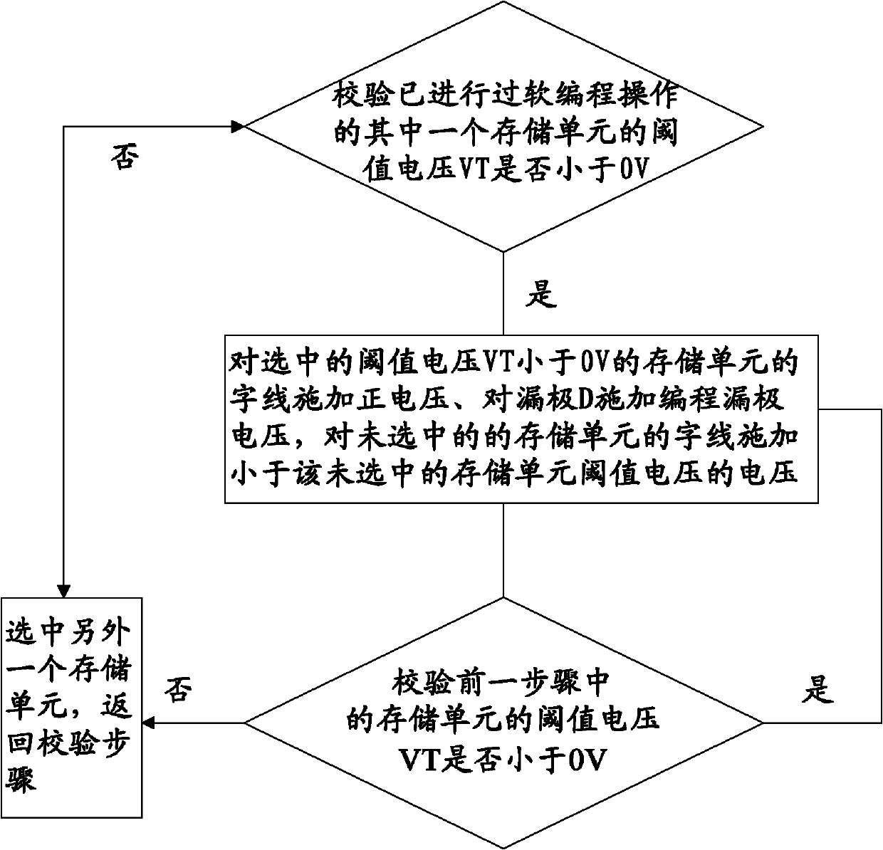
[0044] Please refer to figure 1 , showing a first embodiment of a non-volatile memory over-erasing processing method of the present invention, including the following steps:

[0045] 101. Verification: Select a memory cell that has undergone a soft programming operation, and verify whether the threshold voltage VT of the selected memory cell is less than 0V, if yes, perform step 102; if not, select another memory cell for calibration test;

[0046] 102. Voltage application: apply a positive voltage to the wordline (wordline, WL) of the selected memory cell whose threshold voltage VT is less than 0V, and apply a programming drain voltage to the drain D, and apply a voltage lower than the unselected memory cell to the wordline of the unselected memory cell. The voltage of the threshold voltage VT of the selected memory cell;

[0047] 103. Verifying again: verifying the threshold voltage V of the memory cell processed in step 102 T Whether it is less than 0V, if so, return to ...

Embodiment 2

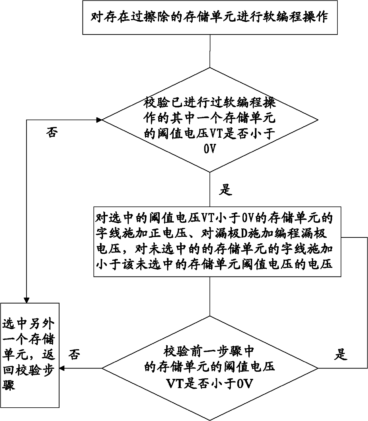
[0051] Please refer to figure 2 , showing a second embodiment of an over-erasing processing method for a non-volatile memory of the present invention, including the following steps:

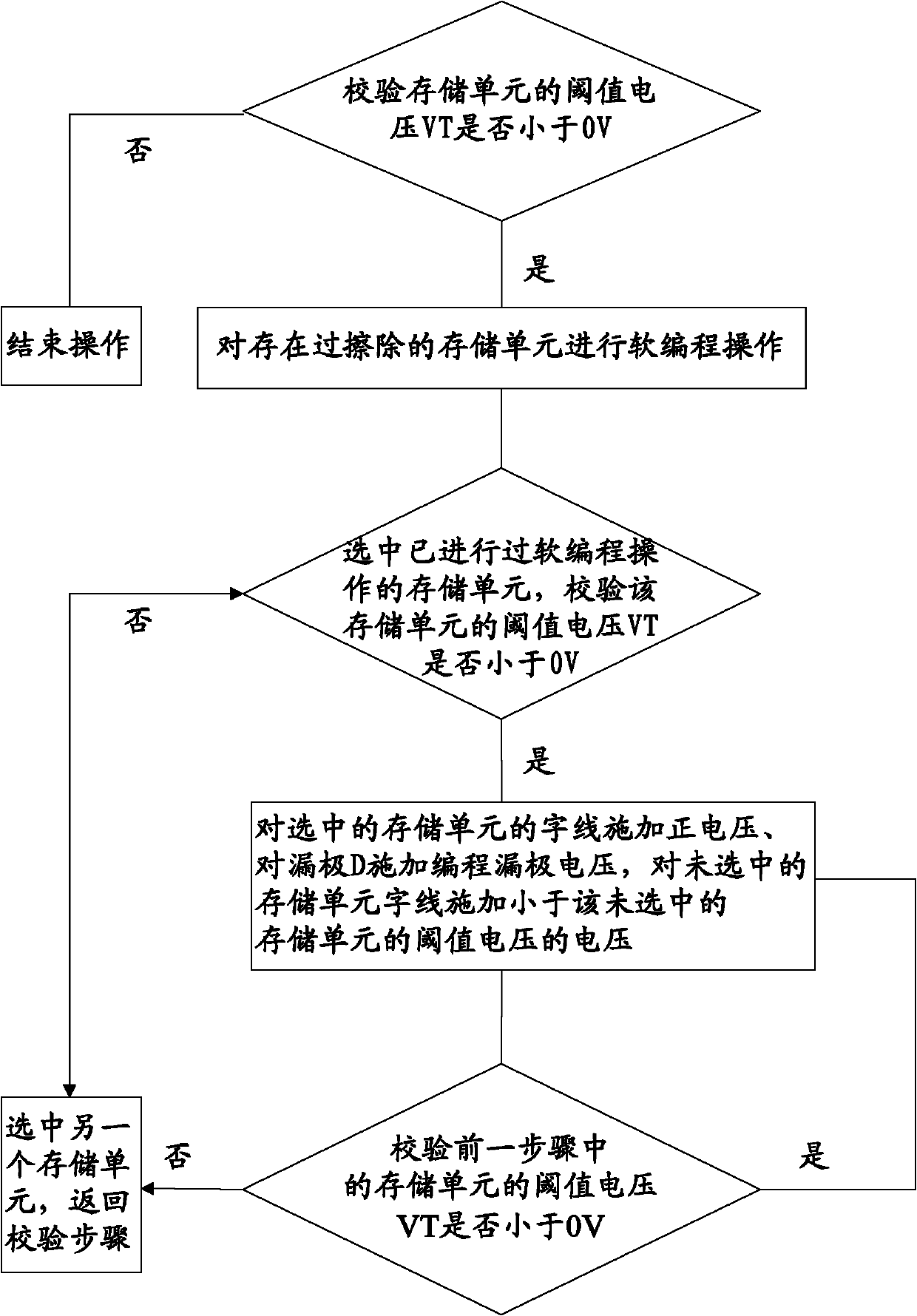
[0052] 201. Soft programming: performing a soft programming operation on memory cells that have been erased;

[0053] 202. Verify: select a memory cell that has undergone a soft programming operation, and verify the threshold voltage V of the selected memory cell T Whether it is less than 0V, if so, then execute step 203; if not, then select another storage unit to verify;

[0054] 203. Voltage application: for the selected threshold voltage V T Apply a positive voltage to the wordline (wordline, WL) of the memory cell less than 0V, apply a programming drain voltage to the drain D, and apply a threshold voltage less than or equal to the threshold voltage V of the unselected memory cell to the wordline of the unselected memory cell T voltage;

[0055] 204, check again: check the threshold vol...


PUM


Abstract

The invention provides an over-erasing processing method for a nonvolatile memory. The method comprises the following steps: checkout: selecting a memory cell, and checking whether the threshold value voltage of the selected storage unit is less than 0V or not; if yes, performing the following steps, and if not, selecting another memory cell to check; voltage application: applying positive voltage to the word line of the selected memory cell, applying programming drain electrode voltage to a drain electrode, applying voltage less than the threshold value voltage of the non-selected memory cell to the word line of the non-selected memory cell; secondary checkout: checking whether the threshold value voltage of the memory cell processed in the voltage application step is less than 0V or not; if yes, returning back to the voltage application step; and if no, finishing the processing. The over-erasing processing method for a nonvolatile memory is characterized in that the memory cell of which the threshold value voltage is less than 0V is subjected to secondary over-erasing processing to guarantee the accuracy of the over-erasing processing. The invention also provides an over-erasing processing system for the nonvolatile memory.

Description

technical field [0001] The invention relates to the technical field of semiconductor memory, in particular to an over-erasing processing method and processing system of a non-volatile memory. Background technique [0002] In order to verify the correctness of memory products, a series of testing procedures will be carried out before the products leave the factory. These storage products may include non-volatile memory products (for example, flash memory Flash, or electrically erasable programmable read-only memory EEPROM, etc.), and may also include one-time programmable OTP memory. The general test process can include product pin (pin) short circuit / open circuit test, logic function test, electrical erasing characteristic test (to determine whether the data in the volatile memory can be electrically erased and rewritten with new data) , program code test (read the program code written into the non-volatile memory and compare it with the written program code to determine wh...

Claims


Application Information

Patent Timeline
Patent Type & Authority Applications(China)
IPC IPC(8): G11C16/34
Inventor 苏志强舒清明
Owner GIGADEVICE SEMICON (BEIJING) INC
Why Eureka
Try Eureka