Device structure conducive to eliminating U-shaped nickel silicide and corresponding technology thereof

A technology of nickel silicide and device structure, which is applied in semiconductor devices, semiconductor/solid-state device manufacturing, electrical components, etc., and can solve problems such as chamfering and voids

Active Publication Date: 2015-06-17
SHANGHAI HUALI MICROELECTRONICS CORP
View PDF2 Cites 0 Cited by
  • Summary
  • Abstract
  • Description
  • Claims
  • Application Information

AI Technical Summary

Problems solved by technology

[0003] The invention provides a device structure and its corresponding process that help to eliminate U-shaped nickel silicides, effectively solving the problems of chamfering and voids caused by existing U-shaped nickel silicides

Method used


Image

  • Device structure conducive to eliminating U-shaped nickel silicide and corresponding technology thereof
  • Device structure conducive to eliminating U-shaped nickel silicide and corresponding technology thereof
  • Device structure conducive to eliminating U-shaped nickel silicide and corresponding technology thereof

Examples


Embodiment approach

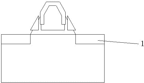
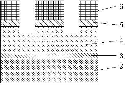
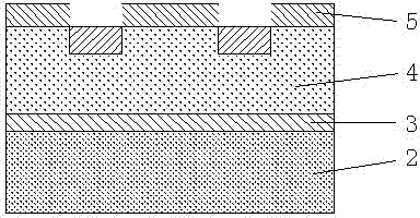
[0030] Please continue to see Figure 2 to Figure 4 shown. In the first step, thin film deposition is performed on polysilicon 4, and then photoresist is spin-coated, and then the silicon oxide layer is opened by dry etching. That is, through flim stack deposition + PR patterning + dry etching (oxide open) to achieve such as figure 2 It is shown with an oxide 5 and a PR layer 6 respectively on polysilicon 4 . In the second step, the photoresist layer 6 on the polysilicon 4 is removed, and then high-temperature oxidation treatment is performed. That is, through PR remove + oxidation to achieve such as image 3 The polysilicon 4 shown, and the photoresist layer 6 is removed. In the third step, the polysilicon gate is etched on the polysilicon 4, and then the oxide 5 is removed. That is, through normal poly etching + oxide strip to achieve such as Figure 4 Polysilicon 4 shown. By first molding the gate with a partially grooved top, a gate nickel silicide with a straight ...


PUM


Abstract

The invention discloses a device structure conducive to eliminating U-shaped nickel silicide and a corresponding technology thereof. The device structure comprises polycrystalline silicon; the top of the polycrystalline silicon is locally grooved; the grooving technology adopts a new photomask and forms a grid by single imaging and etching formation; and when nickel reacts with the polycrystalline silicon to form a silicide, a grid nickel silicide with flat morphology is finally formed. Through the device structure conducive to eliminating U-shaped nickel silicide and the corresponding technology thereof disclosed by the invention, the grid nickel silicide with flat morphology is finally formed by a method of forming a grid locally grooved at the top of the polycrystalline silicon.

Description

technical field [0001] The invention relates to the technical field of semiconductor manufacturing, in particular to a device helpful for eliminating U-shaped nickel silicide. Background technique [0002] In the existing nickel silicide structure, the process of side wall molding is often used. However, during the sidewall forming process (dry etching) it is very easy to cause gate chamfering, and at the same time, the oxide between the gate and the sidewall will form a certain depth of cavity during the integration process. figure 1 For existing nickel silicides using the sidewall molding process, see figure 1 shown. In fact, when nickel and polysilicon react to form silicide, nickel is the one that moves, so the final gate nickel silicide (NiSi) can easily take on an inverted U shape. Contents of the invention [0003] The invention provides a device structure and a corresponding process for eliminating U-shaped nickel silicides, and effectively solves the problems o...

Claims


Application Information

Patent Timeline
Patent Type & Authority Patents(China)
IPC IPC(8): H01L21/28H01L21/285
Inventor 郑春生张文广徐强陈玉文
Owner SHANGHAI HUALI MICROELECTRONICS CORP
Why Eureka
Try Eureka