Partial SOI (Silicon On Insulator) transverse double-diffused device

A lateral double diffusion, device technology, applied in the direction of semiconductor devices, electrical components, circuits, etc., can solve the problems of reducing the area of ​​​​the isolation area, limiting limitations, and limiting the development of self-heating effects.

Active Publication Date: 2012-07-11
SICHUAN CHANGHONG ELECTRIC CO LTD
View PDF5 Cites 4 Cited by
  • Summary
  • Abstract
  • Description
  • Claims
  • Application Information

AI Technical Summary

Problems solved by technology

[0003] SOI (Silicon on Insulator) technology is known as "silicon integrated circuit technology in the 21st century". It is one of the mainstream technologies of the new generation of integrated circuits. The LOCOS process is used for the full dielectric isolation device. The thin-film SOI is isolated by the LOCOS process. There is no well preparation, and the formation of silicon islands can be realized by local oxidation, which greatly reduces the area of ​​the isolation region. However, the vertical withstand voltage of conventional SOI devices It is only determined by the drift region and the buried oxide layer, and its serious self-heating effect limits its development. Park et al. proposed a partial SOI device structure. Due to the existence of silicon windows, the drift region is connected to the substrate, and the depletion layer is connected to the substrate. The bottom extension makes the substrate bear part of the withstand voltage after depletion, which increases the vertical withstand voltage length of the device, and with the decrease of the substrate concentration, the vertical withstand voltage further increases, and the breakdown voltage of the SOI device is changed from the vertical and lateral voltages The smaller one determines that in order to increase the breakdown voltage of conventional SOI devices, the withstand voltage layer is completely depleted, and the doping of the drift region must be low. The vertical withstand voltage is determined by the thickness of the drift region and the buried oxide layer under the drain end surface. The thickness of the drift region from the source to the drain is the same, and the surface electric field is not optimized. Although some SOI devices break the limitation of the vertical withstand voltage of conventional SOI, the surface electric field must satisfy the principle of RESURF, and the surface field will appear high at both ends. The middle low distribution shape makes the drift region of the second-type impurity device not fully optimized, and the limitations of RESURF itself limit the electric field modulation in the drift region, so that the electric field distribution in the drift region of the second-type impurity device cannot be improved, such as figure 1 As shown, a conventional SOI device includes a source, a drain, a first-type impurity substrate 1, a buried oxide layer 2, and a second-type impurity top-layer silicon layer 3, and the second-type impurity top-layer silicon layer 3 includes a first-type impurity Back gate contact region 7, source second-type impurity ohmic contact region 6, second-type impurity device drift region 5, and drain second-type impurity ohmic contact region 4, the first-type impurity substrate 1 is arranged on a horizontal plane , the buried oxide layer 2 is arranged on the first-type impurity substrate 1, the second-type impurity device drift region 5 is arranged on the buried oxide layer 2, and the buried oxide layer 2 connects the first-type impurity substrate 1 and the second-type impurity top layer The silicon layer 3 is electrically isolated, the first-type impurity back gate contact region 8 and the source second-type impurity ohmic contact region 7 are juxtaposed, and are arranged on the upper surface of the second-type impurity device drift region 5 and is close to the source. Drain second-type impurity ohmic contact region 4 is set on the upper surface of second-type impurity device drift region 5 near the drain, wherein the first-type impurity is p-type impurity or n-type impurity, and the second-type impurity is n-type impurity or p-type impurity

Method used


Image

  • Partial SOI (Silicon On Insulator) transverse double-diffused device
  • Partial SOI (Silicon On Insulator) transverse double-diffused device
  • Partial SOI (Silicon On Insulator) transverse double-diffused device

Examples


Embodiment

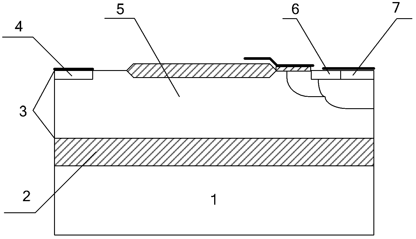
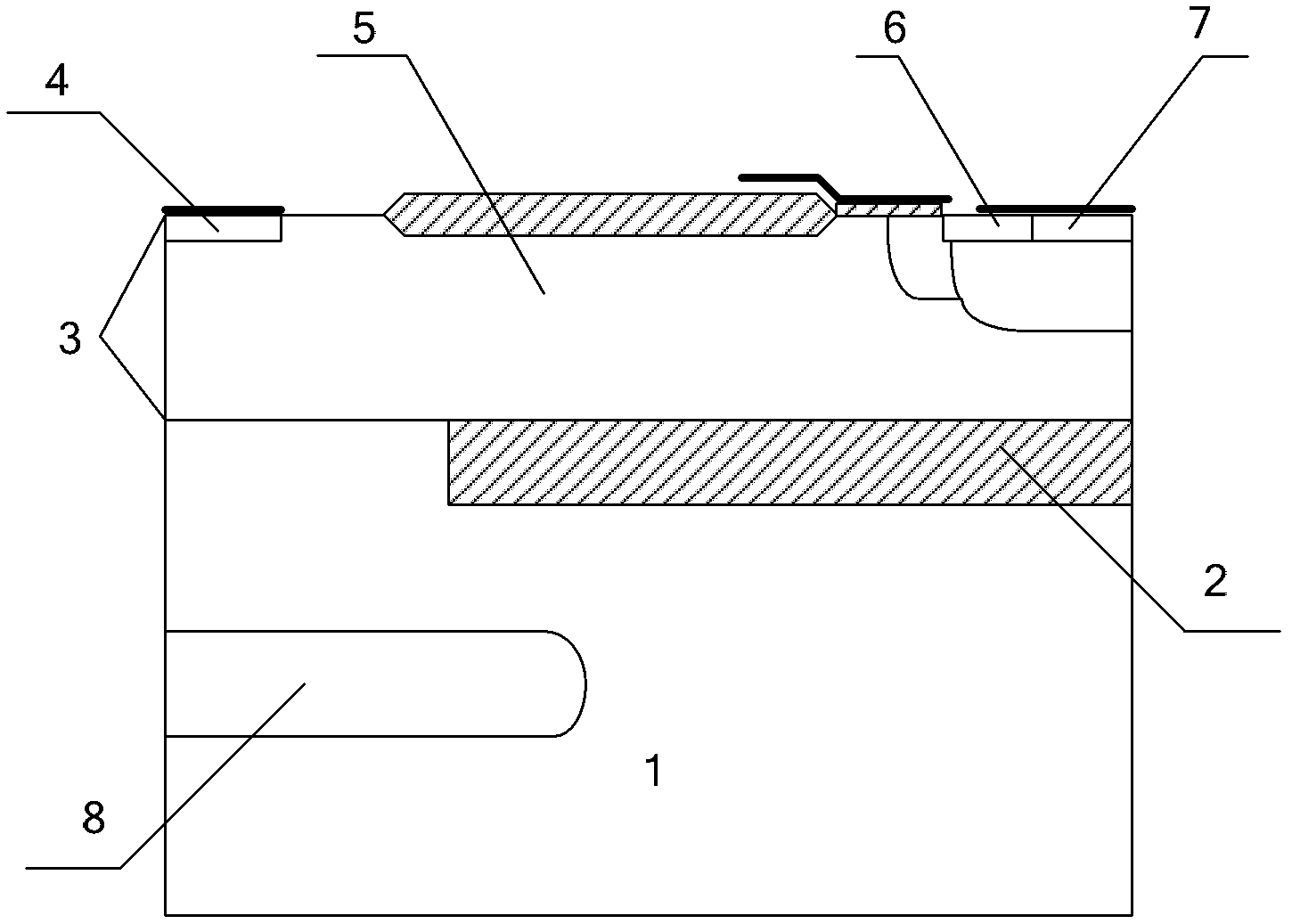
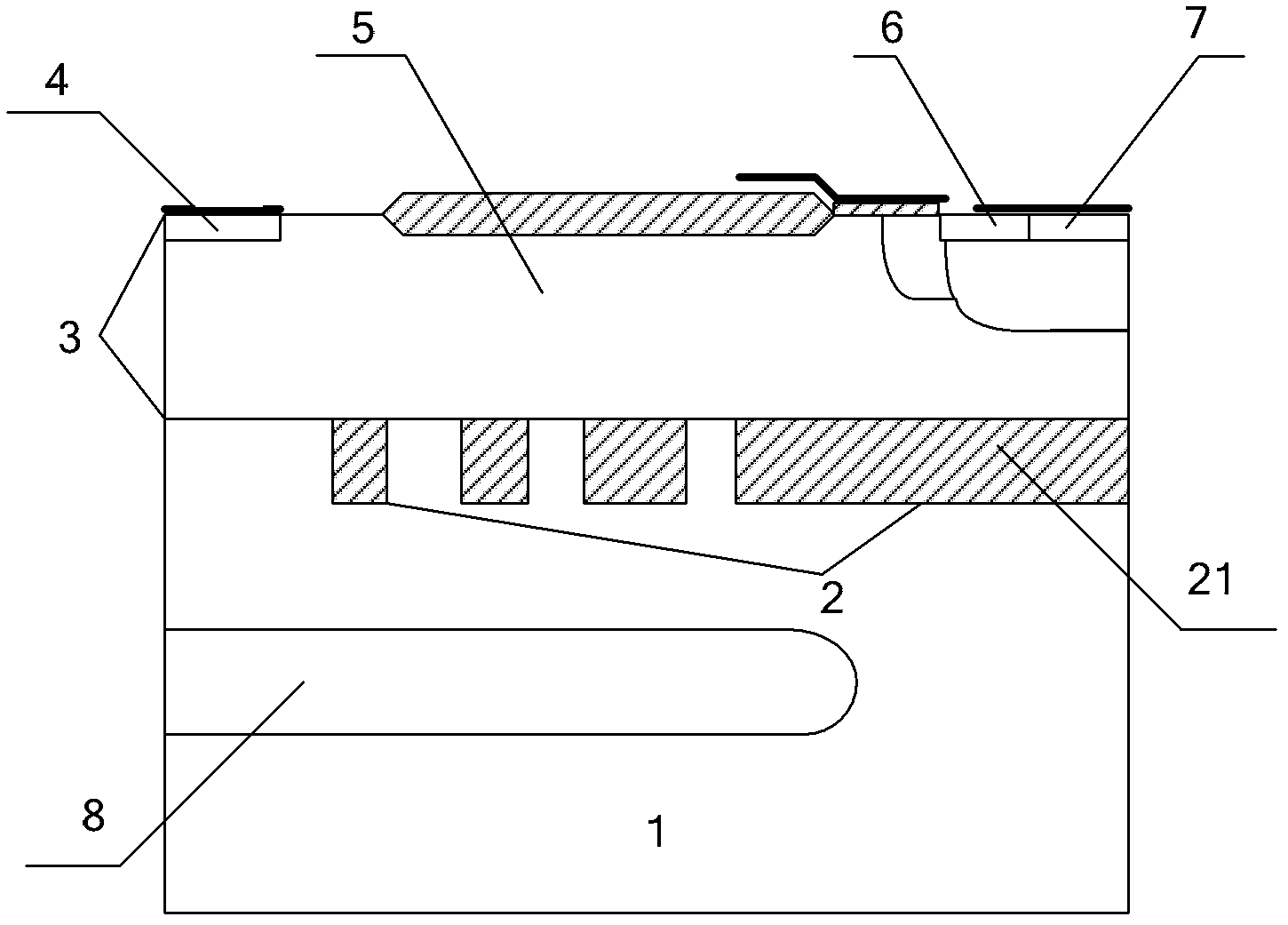
[0025] The buried oxide layer 2 of the partial SOI lateral double-diffusion device in this example can be a continuous layer or discontinuously divided into n segments, and the cross-sectional view when the buried oxide layer is continuous is as follows figure 2 , the cross-sectional view when the buried oxide layer is divided into n segments from one end of the source to the end near the drain is as follows image 3 , the distribution of equipotential lines when a conventional SOI device breaks down is shown in Figure 4 , the distribution diagram of equipotential lines during the breakdown of some SOI lateral double-diffusion devices in this embodiment is as follows Figure 5 , the lateral surface field distribution characteristic curves when the conventional SOI device and the partial SOI lateral double-diffused device of this embodiment break down are as follows Figure 6 , the vertical electric field distribution characteristic curves of the conventional SOI device and ...


PUM


Abstract

The invention relates to SOI technology. The invention provides a partial SOI (Silicon On Insulator) transverse double-diffused device, which solves the problem of obvious self-heating effect in the traditional SOI device. The technical scheme can be summarized as follows: in the partial SOI transverse double-diffused device, one end of a buried oxide layer is positioned below a source and contacts with the edge of the device; the horizontal distance between the other end of the buried oxide layer and a type II impurity ohmic contact region of a drain is not less than zero; and between the other end of the buried oxide layer and the device edge below the drain, a type I impurity substrate and a type II impurity top silicon layer are in contact with each other to form a PN junction. The partial SOI transverse double-diffused device provided by the invention has the following advantages that the thermal generated by the SOI device can be effectively transmitted because the buried oxide layer is open below the drain and is suitable for SOI devices.

Description

[0001] This application is a divisional application of a patent application with the application number 201010579250.7 and the application date is December 8, 2010, and the title is a partial SOI lateral double-diffusion device. technical field [0002] The invention relates to SOI technology, in particular to an SOI lateral double-diffusion device. Background technique [0003] SOI (Silicon on Insulator) technology is known as "silicon integrated circuit technology in the 21st century". It is one of the mainstream technologies of the new generation of integrated circuits. The LOCOS process is used for the full dielectric isolation device. The thin-film SOI is isolated by the LOCOS process. There is no well preparation, and the formation of silicon islands can be realized by local oxidation, which greatly reduces the area of ​​the isolation region. However, the vertical withstand voltage of conventional SOI devices It is only determined by the drift region and the buried oxi...

Claims


Application Information

Patent Timeline
Patent Type & Authority Applications(China)
IPC IPC(8): H01L29/06H01L29/78
Inventor 廖红罗波
Owner SICHUAN CHANGHONG ELECTRIC CO LTD
Why Eureka
Try Eureka