Spot testing method for light emitting diode chip

A technology of light-emitting diodes and chips, which is applied in semiconductor/solid-state device testing/measurement, semiconductor devices, electrical components, etc., can solve the problems of low spot measurement efficiency of LED chip testing machines, affecting the production capacity of light-emitting diodes, etc., and achieve saving optical parameters The effect of testing time, reducing production costs, and improving machine productivity

Active Publication Date: 2012-07-11
ANHUI SANAN OPTOELECTRONICS CO LTD
View PDF5 Cites 10 Cited by
  • Summary
  • Abstract
  • Description
  • Claims
  • Application Information

AI Technical Summary

Problems solved by technology

The response speed is fast when measuring electrical parameters, but the measurement of optical parameters needs to set the chip stabilization time according to the characteristics of the LED chip, the exposure time of the optical measurement system, and use the system function algorithm of calculation correction to obtain the measured value. The time of optical parameters accounts for about 1 / 3~1 / 2 of the total measurement time, which results in low spot measurement efficiency of LED wafer testing machines, which in turn seriously affects the production capacity of light emitting diodes

Method used


Image

  • Spot testing method for light emitting diode chip
  • Spot testing method for light emitting diode chip
  • Spot testing method for light emitting diode chip

Examples


Embodiment Construction

[0025] The implementation of the present invention will be described in detail below in conjunction with the accompanying drawings and examples, so as to fully understand and implement the process of how to apply technical means to solve technical problems and achieve technical effects in the present invention. It should be noted that, as long as there is no conflict, each embodiment and each feature in each embodiment of the present invention can be combined with each other, and the formed technical solutions are all within the protection scope of the present invention.

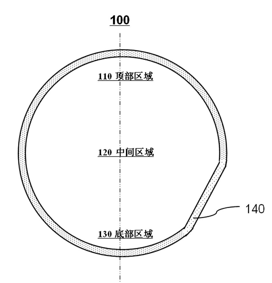
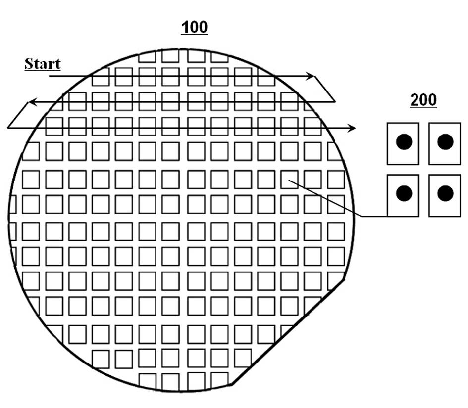
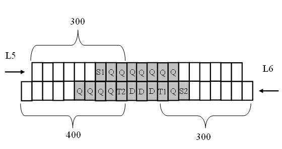
[0026] The following is to distinguish the full test method of the photoelectric parameters of the existing LED chips, and the test method of the full test of the photoelectric parameters and the single test of the electrical parameters is called the new spot test method. Unless otherwise specified in the full text, the new point measurement method refers to the combination of full measurement of photoelectri...


PUM


Abstract

The invention discloses a spot testing method for a light emitting diode, which comprises an optical parameter test and an electric property parameter test. The spot testing method is characterized in that photoelectric parameter full test is performed on chips in a region with scattered optical parameter distribution, and only an electric property parameter single test is performed on the chips in a region with concentrated optical parameter distribution. Under the premise of not increasing any hardware cost, regions with better and concentrated optical parameter distribution of a light emitting diode can be found and distinguished automatically, only electric property parameters are tested, the time for testing optical parameters is saved, the testing rate is improved obviously, the machine productivity is improved greatly, and the manufacturing cost is greatly lowered.

Description

technical field [0001] The invention relates to a spot testing method for a light-emitting diode chip, in particular to a testing method for an aluminum gallium indium phosphorus-based light-emitting diode chip. Background technique [0002] As aluminum gallium indium phosphorus-based light-emitting diodes (light-emitting diodes, LEDs) are widely used in different fields such as display screens, indicator lights, digital products, and backlight sources, objectively, the demand for LEDs has shown a geometric progression. The production efficiency puts forward higher requirements. At present, the electrical and optical parameters of the LED chip need to be measured during the point test. The traditional full point test method uses the ink spot test, that is, the full test of the photoelectric parameters of each chip in the chip (usually WLD, LOP, VF, IR etc.), spray the core particles that do not meet a certain parameter specification range with ink dots for marking, and then...

Claims


Application Information

Patent Timeline
Patent Type & Authority Applications(China)
IPC IPC(8): H01L33/00H01L21/66
Inventor 赖余盟李水清蔡坤煌章小飞
Owner ANHUI SANAN OPTOELECTRONICS CO LTD
Why Eureka
Try Eureka