Light emitting diode structure
A technology of light-emitting diodes and metal electrodes, which is applied in the direction of electrical components, circuits, semiconductor devices, etc., can solve the problems of reduced luminous efficiency and reduced luminous efficiency, and achieve the effects of reducing light, improving luminous efficiency, and improving light
- Summary
- Abstract
- Description
- Claims
- Application Information
AI Technical Summary
Problems solved by technology
Method used
Image

Examples
Embodiment Construction
[0049] In order to have a further understanding and understanding of the structural features of the present invention and the achieved effects, the preferred embodiments and accompanying drawings are used for a detailed description, as follows:
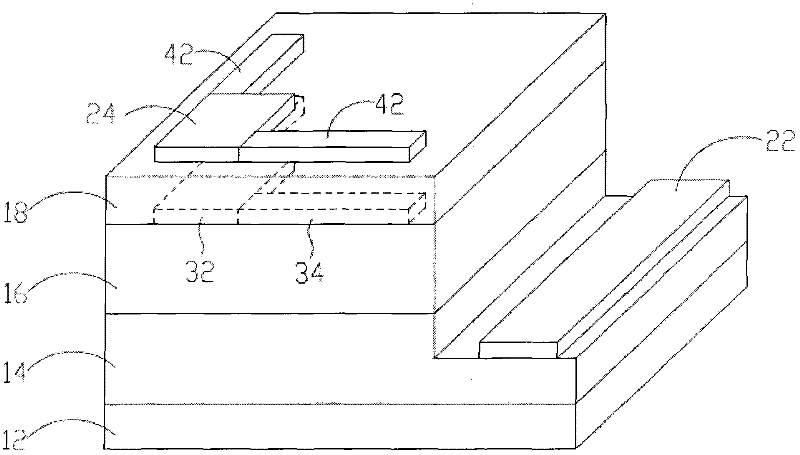
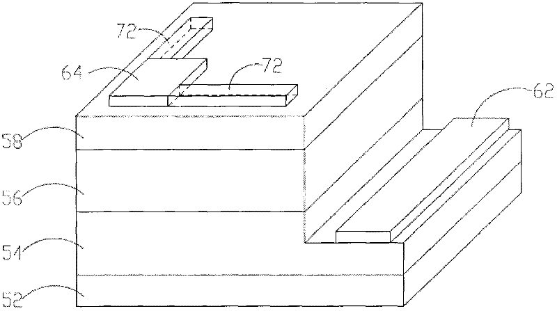
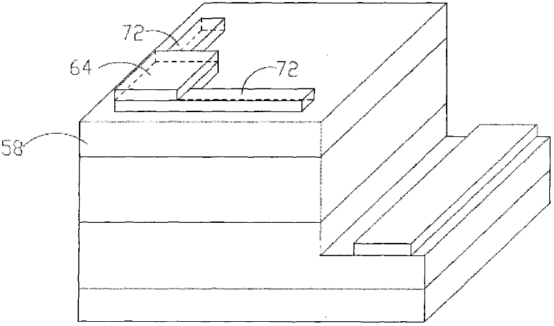
[0050] see figure 2, which is a structural schematic diagram of a light emitting diode structure in a preferred embodiment of the present invention; as shown in the figure, the light emitting diode structure of the present invention includes a substrate 52, a first semiconductor layer 54, a first metal electrode 62, a second The semiconductor layer 56, a conductive layer 58, a second metal electrode 64 and at least one light-transmitting conductive extension 72, the first semiconductor layer 54 is disposed above the substrate 52, the first metal electrode 62 is disposed above the first semiconductor layer 54, The second semiconductor layer 56 is arranged above the first semiconductor layer 54 and adjacent to the first metal electrode...
PUM
 Abstract
Description
Claims
Application Information
 - Generate Ideas
- Intellectual Property
- Life Sciences
- Materials
- Tech Scout
- Unparalleled Data Quality
- Higher Quality Content
- 60% Fewer Hallucinations
Browse by: Latest US Patents, China's latest patents, Technical Efficacy Thesaurus, Application Domain, Technology Topic, Popular Technical Reports.
© 2025 PatSnap. All rights reserved.Legal|Privacy policy|Modern Slavery Act Transparency Statement|Sitemap|About US| Contact US: help@patsnap.com