
Semiconductor package and fabrication method thereof

A manufacturing method and packaging technology, which are applied in semiconductor/solid-state device manufacturing, semiconductor device, semiconductor/solid-state device components and other directions, can solve problems such as short circuit of electrical contact pads 100, and achieve the effect of avoiding short circuit

Active Publication Date: 2014-07-16
SILICONWARE PRECISION IND CO LTD
View PDF3 Cites 0 Cited by
  • Summary
  • Abstract
  • Description
  • Claims
  • Application Information

AI Technical Summary

Problems solved by technology

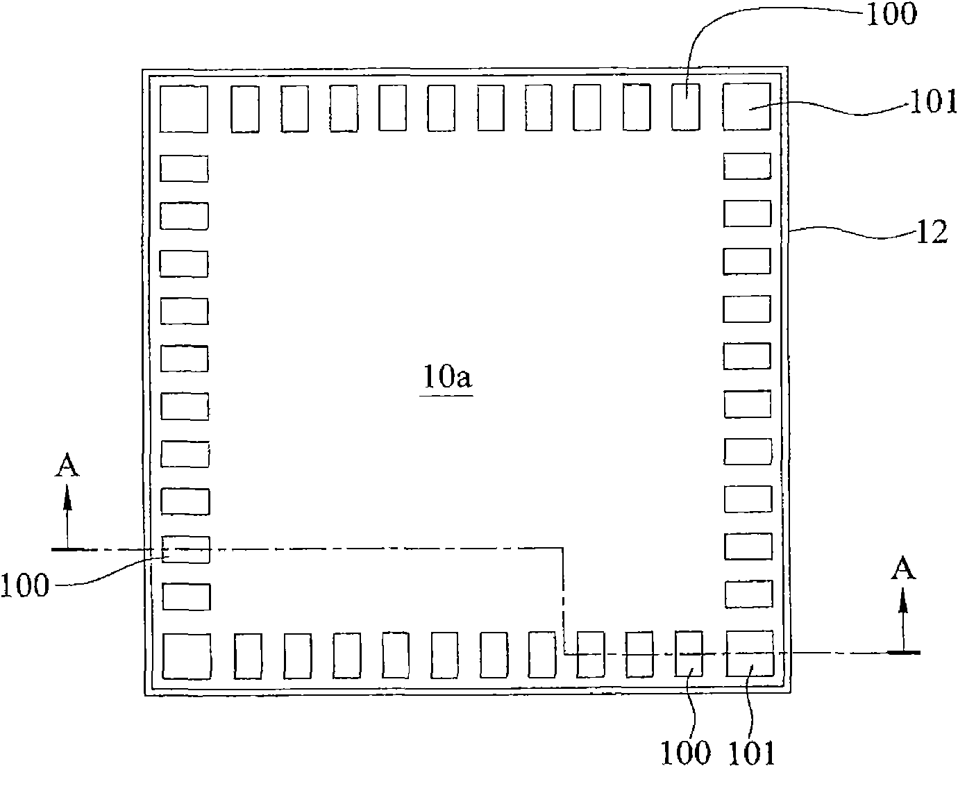
[0007] However, if Figure 1C As shown, in the subsequent manufacturing method, when the package is arranged on the circuit board 5, each of the electrostatic discharge protection pads 101 and the electrical contact pads 100 are combined to the circuit board 5 through solder bumps 4, and then soldered , the solder bumps 4 on the electrical contact pads 100 at the edge of the substrate unit 10 are likely to bridge to the metal layer 12 on the side surface 10c of the substrate unit 10, resulting in a short circuit between the electrical contact pads 100
In addition, if the material of the metal layer 12 is a solderable material, the situation that the electrical contact pad 100 bridges with the metal layer 12 to cause a short circuit is even more serious.

Method used


Image

  • Semiconductor package and fabrication method thereof
  • Semiconductor package and fabrication method thereof
  • Semiconductor package and fabrication method thereof

Examples


Embodiment Construction

[0046] Embodiments of the present invention are described below through specific examples, and those skilled in the art can easily understand other advantages and effects of the present invention from the content disclosed in this specification.

[0047] It should be noted that the structures, proportions, sizes, etc. shown in the drawings attached to this specification are only used to match the content disclosed in the specification, for those skilled in the art to understand and read, and are not used to limit the implementation of the present invention. condition, so it has no technical substantive meaning, and any modification of structure, change of proportional relationship or adjustment of size shall still fall within the scope of the present invention without affecting the effect and purpose of the present invention. The disclosed technical content must be within the scope covered. At the same time, terms such as "top", "upper", "one" and "lower" quoted in this specif...


PUM


Abstract

A semiconductor package is provided, which includes a substrate unit having conductive pads and ESD protection pads formed on a bottom surface thereof; an encapsulant covering a top surface of the substrate unit; and a metal layer disposed on a top surface of the encapsulant and having connecting extensions formed on side surfaces of the substrate unit and the encapsulant for electrically connecting the ESD protection pads, wherein portions of the side surfaces of the substrate unit corresponding in position to the conductive pads are exposed from the metal layer so as to ensure that solder bumps subsequently formed to connect the conductive pads of the semiconductor package to a circuit board are not in contact with the metal layer, thereby effectively avoiding the risk of short circuits.

Description

technical field [0001] The invention relates to a semiconductor package and its manufacturing method, in particular to a semiconductor package with a metal layer for preventing short circuit and preventing electromagnetic wave interference and its manufacturing method. Background technique [0002] With the evolution of semiconductor technology, semiconductor products have developed different packaging product types, and in order to improve electrical quality, many semiconductor products have a shielding function to prevent electromagnetic interference (EMI). [0003] At present, in semiconductor packages, a metal layer is plated on the entire top surface and side surfaces of the package, and the metal layer on the side surface is connected to the ground plane (Ground plane) of the circuit board to achieve EMI barrier (Shielding) )Effect. [0004] However, generally, no circuit is designed on the side of the semiconductor package. If additional circuits are required to cond...

Claims


Application Information

Patent Timeline
Patent Type & Authority Patents(China)
IPC IPC(8): H01L23/60H01L23/31H01L21/56H01L21/60
CPCH01L2224/16227H01L2924/3841H05K1/0259H05K3/3436H01L23/3121H01L24/13H01L23/60H01L2224/16225H01L2224/48227H01L2924/3025H01L2224/131H01L24/48H01L24/16H01L2924/00014Y02P70/50H01L2924/014H01L2924/00H01L2224/45099H01L2224/45015H01L2924/207
Inventor 方颢儒钟兴隆钟匡能林建成朱恒正
Owner SILICONWARE PRECISION IND CO LTD
Learn More