

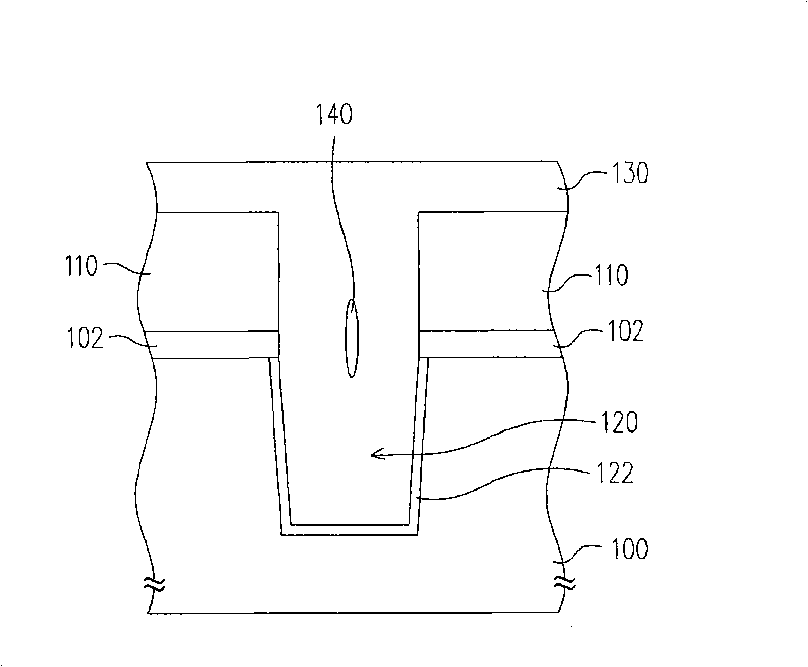
Shallow groove isolation structure and floating grid manufacture method
A manufacturing method and technology of isolation structure, which are applied in semiconductor/solid-state device manufacturing, electrical components, circuits, etc., can solve the problems that the silicon oxide layer 130 cannot be completely filled, the performance of semiconductor components is reduced, and the groove filling ability is poor, and the improvement is achieved. Isolation ability, prevent short circuit, improve the effect of hole problem
- Summary
- Abstract
- Description
- Claims
- Application Information
AI Technical Summary
Problems solved by technology
Method used
Image

Examples
Embodiment Construction
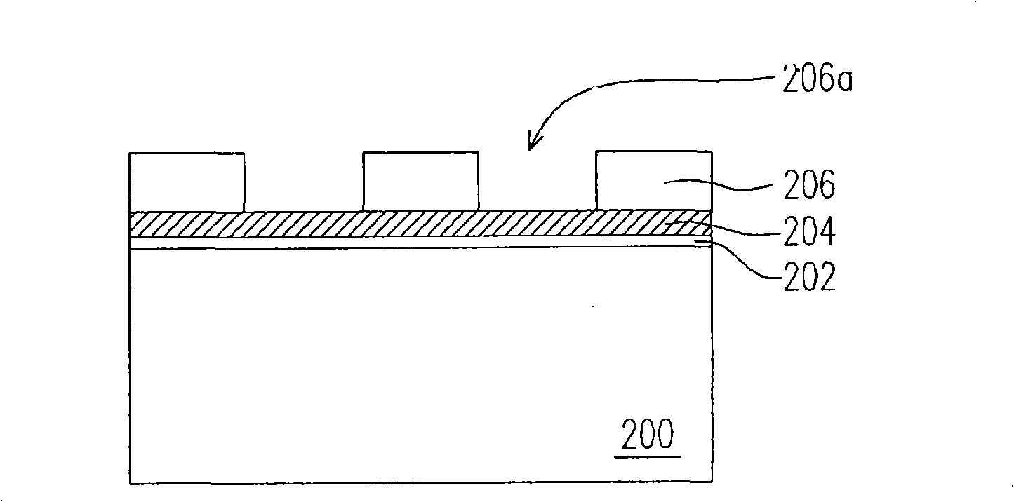
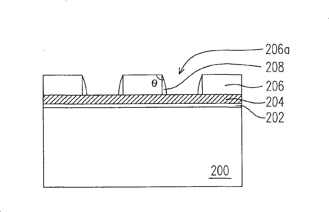
[0051] Figure 2A to Figure 2F The drawing is a cross-sectional view of the manufacturing process of the floating gate according to the embodiment of the present invention.
[0052] First, please refer to Figure 2A , a substrate 200 is provided, and the substrate 200 is, for example, a silicon substrate. For example, conductive regions (not shown) or generally known semiconductor elements (not shown) have been formed in the substrate 200 , but the present invention is not limited thereto. After that, a dielectric layer 202 , a conductive layer 204 and a patterned mask layer 206 are sequentially formed on the substrate 200 . The material of the dielectric layer 202 is, for example, silicon oxide, and its formation method is, for example, chemical vapor deposition or thermal oxidation. The material of the conductor layer 204 is, for example, doped or undoped single crystal silicon, and its formation method is, for example, chemical vapor deposition. The patterned mask layer...
PUM
 Abstract
Description
Claims
Application Information