Data sending method and system on basis of chip

A data transmission method and chip technology, applied in the field of communication, can solve the problems of shrinking size, impact on life, low working accuracy, etc., and achieve the effect of simplifying the peripheral circuit of the chip, guaranteeing the frequency accuracy, and reducing the manufacturing cost.

Inactive Publication Date: 2014-04-09
WUXI ZETAI MICROELECTRONICS
View PDF5 Cites 0 Cited by
  • Summary
  • Abstract
  • Description
  • Claims
  • Application Information

AI Technical Summary

Problems solved by technology

[0003] Because the prior art needs to adopt expensive surface acoustic wave device or crystal oscillator circuit to provide reference reference frequency, therefore, the whole chip manufacturing cost is high; there are many peripheral pins of surface acoustic wave device or crystal oscillator circuit, so that it is necessary to ensure The realization of the function, the peripheral circuit of the surface acoustic wave device or the crystal oscillator circuit is relatively complicated, the size of the whole chip is large, which is not conducive to further integration. In addition, the volume of the surface acoustic wave device or crystal oscillator circuit itself is also large, so that the chip cannot Better integration to reduce the size; the frequency stability of surface acoustic wave devices is not high, and the working accuracy is low; the crystal oscillation circuit provides a reference reference frequency through the principle of mechanical oscillation. In some complex environments, the accuracy of the crystal oscillation circuit There are problems, and the lifespan will also be affected by the environment

Method used


Image

  • Data sending method and system on basis of chip
  • Data sending method and system on basis of chip
  • Data sending method and system on basis of chip

Examples


Embodiment Construction

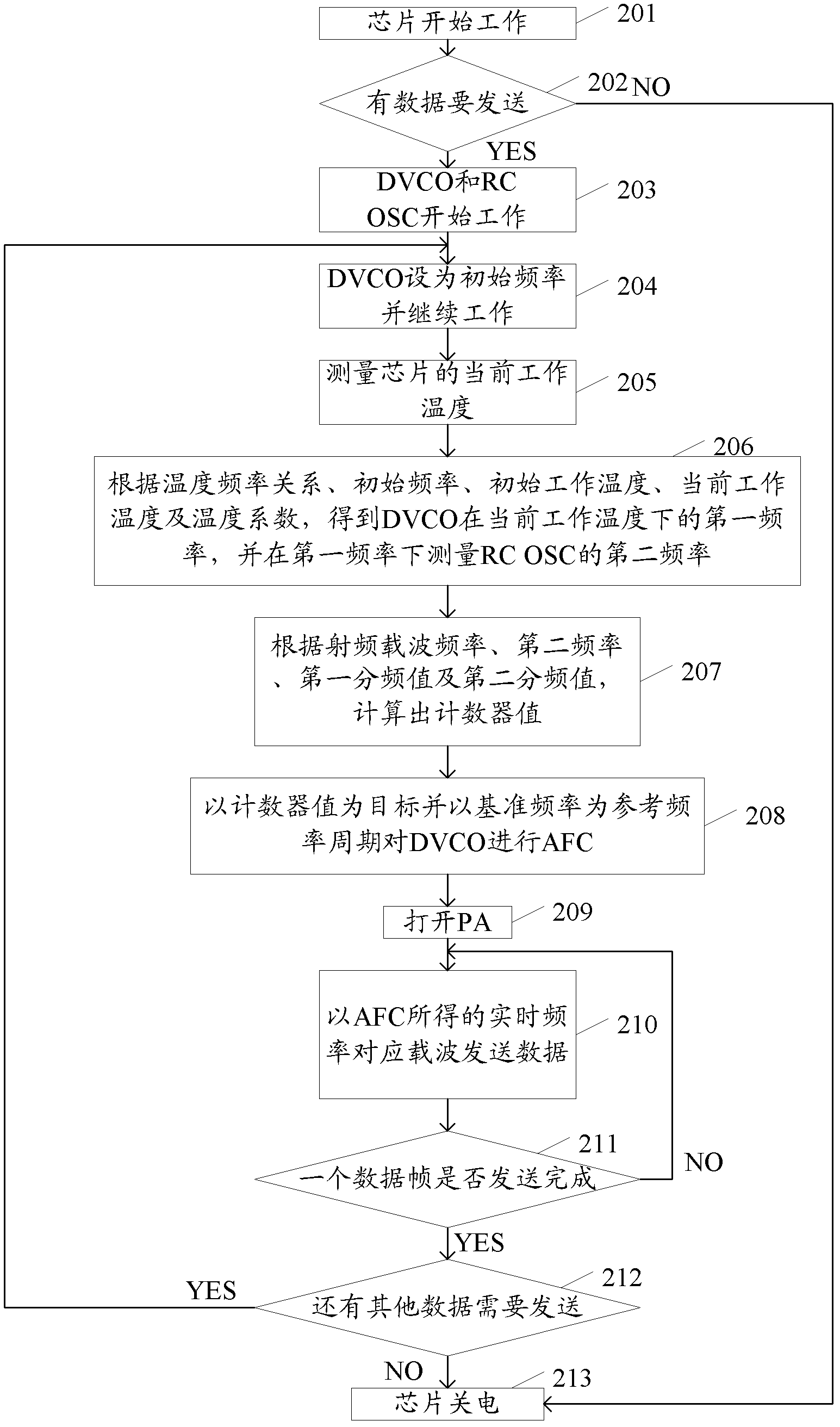
[0047] Embodiments of the present invention will be described in detail below in conjunction with the accompanying drawings.

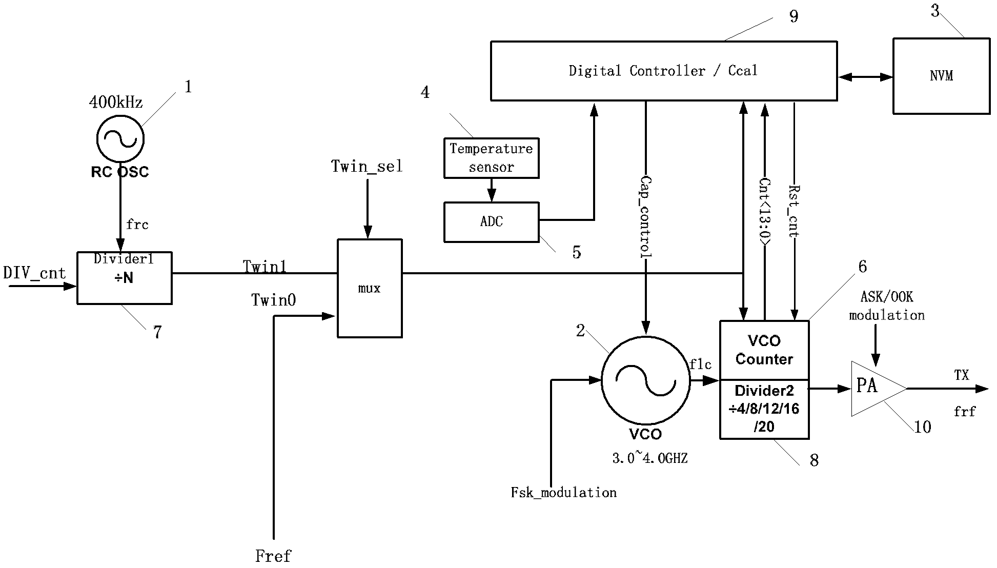
[0048] Such as figure 1 As shown, the data sending system of the first embodiment of the present invention is integrated in one chip, which mainly includes:

[0049] RC OSC (RC Oscillator) 1, which is a low temperature coefficient oscillator with a frequency determined by resistance and capacitance, is mainly used to generate a clock whose cycle can be measured, as the following Digital Voltage Controlled Oscillator (Digital Voltage Controlled Oscillator, DVCO) 2 for automatic frequency control (Automatic Frequency Control, AFC) reference;

[0050] DVCO2, which is a high-frequency LC oscillator, is used to generate the required RF and measure the frequency of the resistance-capacitance oscillator (RC Oscillator, RC OSC) 1, which can complete digital signal control;

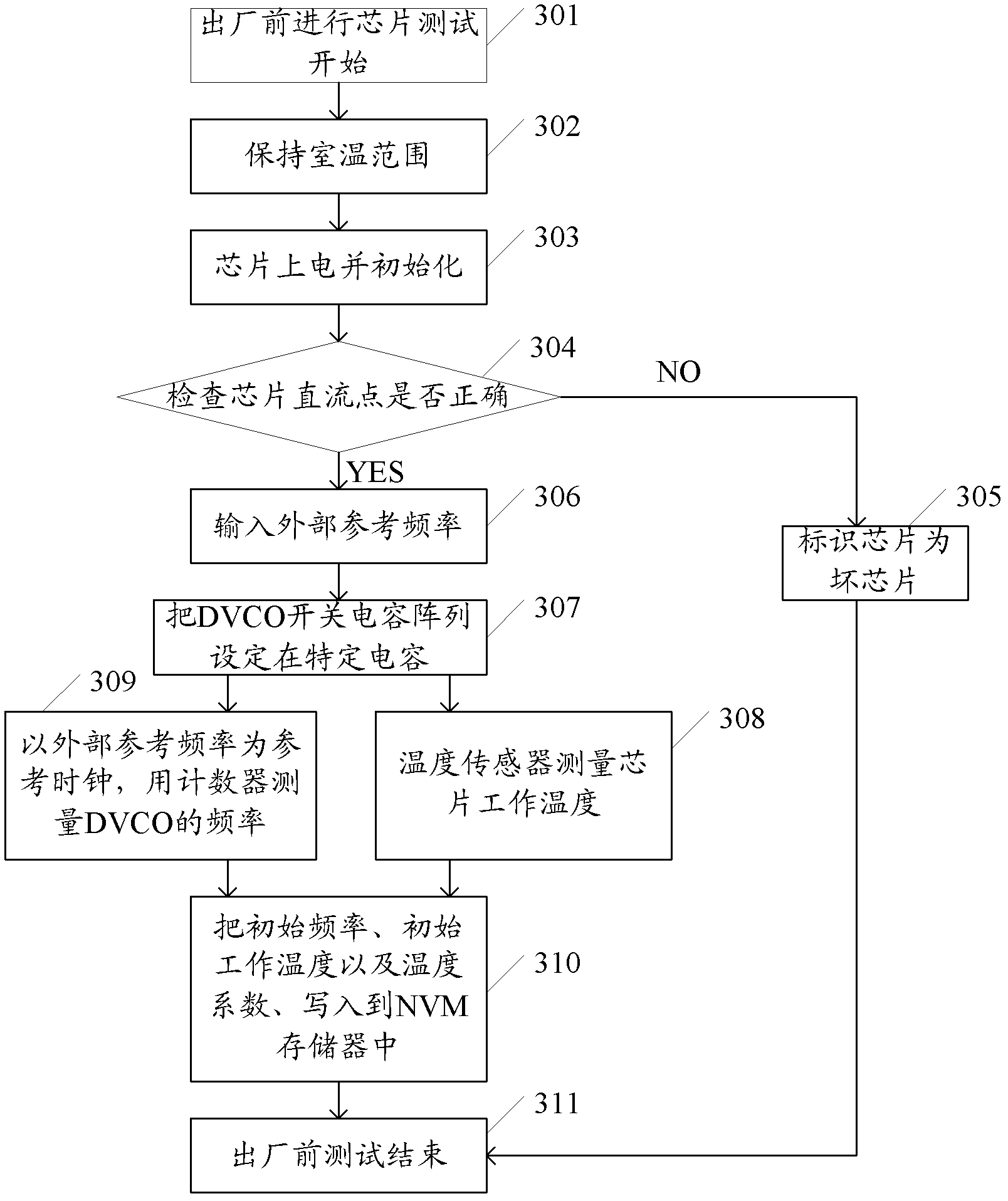
[0051] The storage module 3 is used to store the preset initial frequency flc0 of DV...


PUM


Abstract

The embodiment of the invention discloses a data sending method and system on the basis of a chip. The data sending method comprises the following steps of: according to a preset temperature frequency relation including an initial frequency, initial working temperature and a temperature coefficient, determining the working frequency by the measured current working temperature, further determining reference frequency, determining a counter value which carries out adjustment by adopting radio-frequency carrier frequency as an object, and further sending data corresponding to carrier by the obtained real-time frequency after automatic frequency control. Therefore, according to the data sending method and system disclosed by the embodiment of the invention, the condition that the chip adopts an expensive acoustic surface wave oscillator or a crystal oscillation circuit to provide the referenced reference frequency is avoided, so that the manufacturing cost of the chip is greatly reduced, a peripheral circuit of the chip is simplified, the size of the chip is reduced, further integration is facilitated, the stability of the frequency when the chip works is also guaranteed, the frequency accuracy also can be well ensured under the complex environment, and the service life is prolonged.

Description

technical field [0001] The invention relates to the field of communication, in particular to a chip-based data sending method and system. Background technique [0002] There are generally two ways to send data at present. One is to use a surface acoustic wave oscillator to generate a radio frequency (Radio Frequency, RF), and then adjust the surface acoustic wave device to send frequency shift keying by mixing or using the data to be sent. (Frequency-Shift Keying, FSK) signal, or use switch PA to send amplitude keying (Amplitude-Shift Keying, ASK) or binary on-off keying (On-Off Keying, OOK) signal; the other is to use a crystal oscillator circuit A reference frequency reference is generated as a reference of a phase-locked loop (Phase Locked Loop, PLL) circuit, and then the PLL circuit is used to generate the frequency required by RF and then sent out by the PA. Among them, the FSK data is generally directly modulated through the PLL, and the ASK or OOK data is directly re...

Claims


Application Information

Patent Timeline
Patent Type & Authority Patents(China)
IPC IPC(8): H03L7/18H03L1/02
Inventor 邓建元
Owner WUXI ZETAI MICROELECTRONICS
Why Eureka
Try Eureka