Forming process for fine line circuit with line width being below 0.05mm of flexible printed circuit board

A flexible printing and molding process technology, which is applied in the direction of removing conductive materials by chemical/electrolytic methods, can solve the problem that the process capability is difficult to meet the wiring requirements of IC packaging flexible substrates, and achieve low cost, high pass rate, and simple process Effect

Active Publication Date: 2012-07-18
吉安新宇腾跃电子有限公司
View PDF4 Cites 24 Cited by
  • Summary
  • Abstract
  • Description
  • Claims
  • Application Information

AI Technical Summary

Problems solved by technology

[0002] At present, the ordinary circuit of flexible printed circuit board FPC (Flexible Printed Circuit board) is about 0.075mm, and the process capability is difficult to meet the wiring requirements of IC packaging flexible substrates. 0.03mm, which belongs to the pattern of high-density line wiring

Method used


Image

  • Forming process for fine line circuit with line width being below 0.05mm of flexible printed circuit board
  • Forming process for fine line circuit with line width being below 0.05mm of flexible printed circuit board
  • Forming process for fine line circuit with line width being below 0.05mm of flexible printed circuit board

Examples


Embodiment Construction

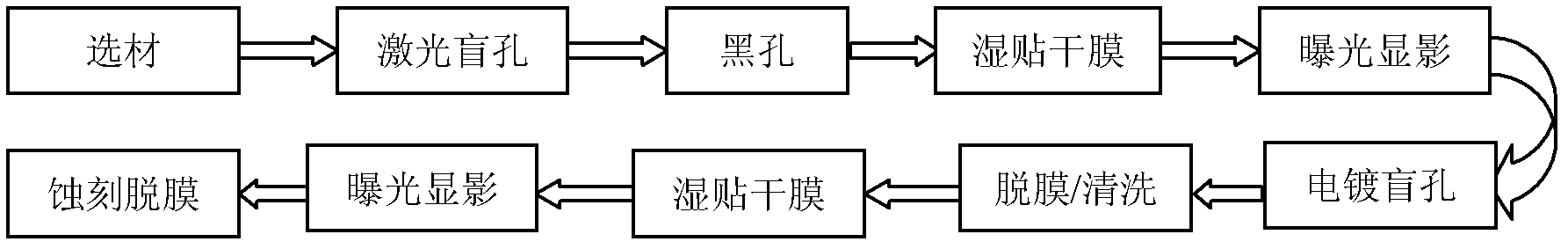
[0018] The present invention will be described in further detail below in conjunction with the accompanying drawings and embodiments. The flexible printed circuit board forming process of the present invention, the process flow is: material selection, laser blind hole, black hole, wet paste dry film, exposure and development, electroplating blind hole, stripping cleaning, wet paste dry film again, exposure and development again, Etched lines. Such as image 3 As shown, the specific steps are:

[0019] 1. Material selection. Copper-clad base material with copper thickness of 9um on both sides and polyimide PI thickness of 20um in the middle is used. The overall size is 250×250-100mm in length, 1 piece. In this embodiment, it is 250×250mm in length.

[0020] 2. Laser drilling blind holes. According to the existing technology, laser drilling blind holes is used on the copper-clad substrate. The hole depth is to drill through the upper copper and the middle PI, and the hole diam...


PUM


Abstract

The invention discloses a forming process for a fine line circuit with line width being below 0.05mm of a flexible printed circuit board, aiming to manufacture an IC (Integrated Circuit) package flexible substrate which has a copper-coated base material with the width being below 40 mu m and is 0.05mm in line width. The forming process for the fine line circuit with the line width being below 0.05mm of the flexible printed circuit board comprises the following steps of: material selecting, laser-based blind hole drilling, hole blacking, wet-process dry film attaching, exposure for development, blind hole electroplating, film removing and cleaning, secondary wet-process dry film attaching, secondary exposure for development, and circuit etching. Compared with the prior art, the IC package flexible substrate, which has the copper-coated base material with the width being below 40 mu m, is 0.05mm in line width and is manufactured through the steps of material selecting, laser-based blind hole drilling, hole blacking, wet-process dry film attaching, exposure for development, blind hole electroplating, film removing and cleaning, secondary wet-process dry film attaching, secondary exposure for development and circuit etching, fully meet a wiring requirement of the IC package flexible substrate, and is simple in process, low in cost, high in qualification rate and suitable for industrialized production.

Description

technical field [0001] The invention relates to a preparation process of a printed circuit board, in particular to a forming process of a flexible printed circuit board. Background technique [0002] At present, the ordinary circuit of flexible printed circuit board FPC (Flexible Printed Circuit board) is about 0.075mm, and the process capability is difficult to meet the wiring requirements of IC packaging flexible substrates. 0.03mm, which belongs to the high-density line wiring pattern. In order to cooperate with the high-density IC packaging process with ultra-thin within 40um and a line width / line spacing process of 0.03mm / 0.03mm, the thickness of the copper base material of the IC packaging flexible substrate needs to be controlled within 40um. The pads of electronic components on IC packaging flexible substrates are getting smaller and smaller. Today's mainstream IC packaging flexible substrates are usually made with Φ0.1mm blind holes corresponding to Φ0.25mm pads. ...

Claims


Application Information

Patent Timeline
Patent Type & Authority Applications(China)
IPC IPC(8): H05K3/06
Inventor 牛勇
Owner 吉安新宇腾跃电子有限公司
Why Eureka
Try Eureka