Reflective GaA1As photoelectric cathode with sensitive peak response at 532nm and preparation method of reflective GaA1As photoelectric cathode
A technology of photocathode and peak response, which is applied in cold cathode manufacturing, electrode system manufacturing, discharge tube/lamp manufacturing, etc. It can solve the problems of narrow-band response noise, inability to use all-weather, wide cathode response band, etc., to reduce interface Effects of recombination rate, reduction of growth interface stress, and improvement of interface properties
- Summary
- Abstract
- Description
- Claims
- Application Information
AI Technical Summary
Problems solved by technology
Method used
Image
Examples
Embodiment 1
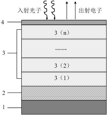
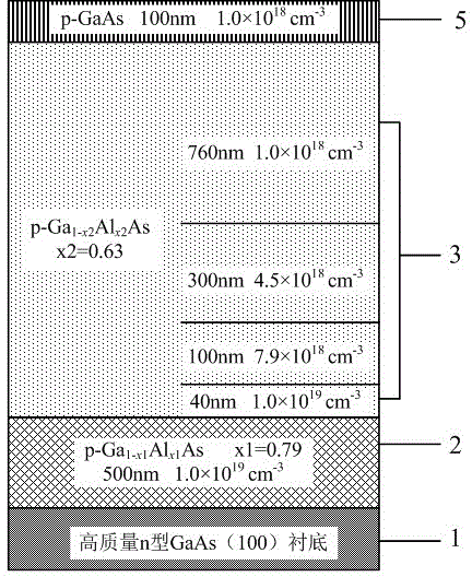
[0041] Step 1: In high quality (dislocation density ≤ 100 cm -2 ) On n-type GaAs(100) substrate 1, p-type doped Ga was grown by MOCVD epitaxy 1-x1 Al x1 As buffer layer 2, Ga 1-x1 Al x1 Al composition value of As buffer layer 2 x 1 is taken as 0.79, the total thickness is taken as 500 nm, the uniform doping method is adopted, the doping atoms are Zn, and the doping concentration is 1.0×10 19 cm -3 .
[0042] Step 2: In Ga 1-x1 Al x1 Epitaxial growth of Ga on As buffer layer 2 1-x2 Al x2 Emitter layer 3 with As doping concentration gradient, Ga 1-x2 Al x2 Al composition value of As emission layer 3 x 2 is taken as 0.63; by 4 p-type Ga 1-x Al x The unit layer composed of As epitaxial material, the thickness value of each unit layer changes according to the index, respectively designed as 40nm, 100 nm, 300 nm, 760 nm, Ga 1-x2 Al x2 The total thickness of the As doping concentration gradient emission layer is 1200 nm; the four units are all doped with Zn, and the ...
Embodiment 2
[0052] The first step: On the n-type GaAs(100) substrate, grow p-type doped Ga by MOCVD epitaxy 1-x1 al x1 As buffer layer, Ga 1-x1 al x1 Al composition value of As buffer layer x 1 is taken as 0.75, the total thickness is taken as 100 nm, the uniform doping method is adopted, the doping atoms are Zn, and the doping concentration is 1.0×10 19 cm -3 .
[0053] Step 2: In Ga 1-x1 al x1 Epitaxial Growth of Ga on As Buffer Layer 1-x2 al x2 Emitter layer with graded As doping concentration, Ga 1-x2 al x2 Al composition value of As emission layer x 2 is taken as 0.68; by 4 p-type Ga 1-x al x The unit layer composed of As epitaxial material, the thickness of each unit layer is designed to be 40nm, 100nm, 300nm, 760nm, Ga 1-x2 al x2 The total thickness of the As doping concentration gradient emission layer is 3000 nm; the four units are all doped with Zn, and the doping concentration of each layer from the bottom to the top is taken as 1.0×10 from the inner surface to ...
Embodiment 3
[0060] The first step: On the n-type GaAs (100) substrate, grow p-type doped Ga by MBE epitaxy 1-x1 al x1 As buffer layer, Ga 1-x1 al x1 Al composition value of As buffer layer x 1 is taken as 0.9, the total thickness is taken as 2000 nm, the uniform doping method is adopted, the doping atoms are Be, and the doping concentration is 1.0×10 19 cm -3 .
[0061] Step 2: In Ga 1-x1 al x1 Epitaxial Growth of Ga on As Buffer Layer 1-x2 al x2 Emitter layer with graded As doping concentration, Ga 1-x2 al x2 Al composition value of As emission layer x 2 is taken as 0.60; by 4 p-type Ga 1-x al x The unit layer composed of As epitaxial material, the thickness of each unit layer is designed to be 10nm, 20nm, 40nm, 80nm, Ga 1-x2 al x2 The total thickness of the As doping concentration gradient emission layer is 150 nm; the four units are all doped with Be, and the doping concentration of each layer from the bottom to the top is taken as 1.0×10 from the inner surface to the o...
PUM
 Abstract
Description
Claims
Application Information


