Heavy doping method of source electrode and drain electrode, semiconductor device and manufacturing method thereof

A heavily doped, semiconductor technology, used in semiconductor/solid-state device manufacturing, semiconductor devices, electrical components, etc., can solve the problems of ineffective reduction of parasitic capacitance, simple steps, etc., to improve frequency response characteristics, reduce Small Miller capacitance, the effect of reducing parasitic overlap capacitance

Inactive Publication Date: 2012-07-25
SHANGHAI HUALI MICROELECTRONICS CORP
View PDF4 Cites 4 Cited by
  • Summary
  • Abstract
  • Description
  • Claims
  • Application Information

AI Technical Summary

Problems solved by technology

The process steps of the prior art are simple but have no substantial effect on reducing parasitic capacitance

Method used


Image

  • Heavy doping method of source electrode and drain electrode, semiconductor device and manufacturing method thereof
  • Heavy doping method of source electrode and drain electrode, semiconductor device and manufacturing method thereof
  • Heavy doping method of source electrode and drain electrode, semiconductor device and manufacturing method thereof

Examples


Embodiment Construction

[0017] In order to make the above objects, features and advantages of the present invention more comprehensible, specific implementations of the present invention will be described in detail below in conjunction with the accompanying drawings.

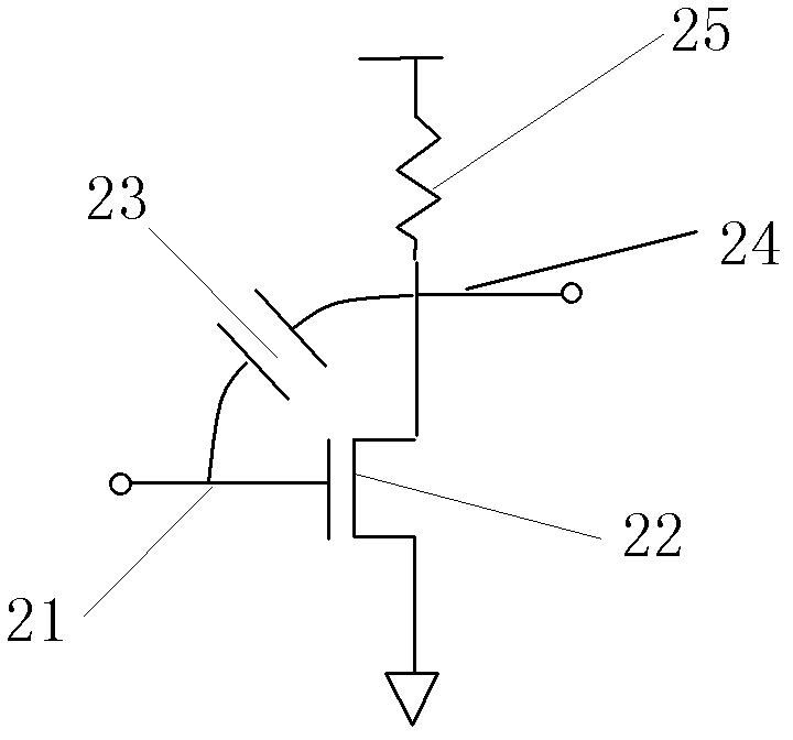
[0018] In the source-drain heavy doping method provided by the embodiment of the present invention, the ion implantation direction of the source-drain heavy doping method is inclined to the source direction and forms an included angle with the direction perpendicular to the substrate. Please refer to Figure 4 , taking the preparation of NMOS transistors in the CMOS device process as an example, a gate structure 41 is first formed on a substrate 44; then, using the gate structure 41 as a mask, a light Doping to form a source extension region and a drain extension region; then forming a gate spacer on the side wall of the gate structure 41; using the gate structure 41 and the gate spacer as a mask to perform heavy source-drain doping ,...


PUM


Abstract

The invention discloses a heavy doping method of a source electrode and a drain electrode. According to the heavy doping method of the source electrode and the drain electrode, the ion implantation direction inclines to the direction of the source electrode and is vertical to the direction of a substrate so as to form an included angle, the heavy doping area of the source electrode and a heavy doping area of the drain electrode are of asymmetrical structures as the ion implantation direction is not vertical to the surface of the substrate, the distance between the heavy doping area of the drain electrode is far from a groove by pulling, and the area of the overlapping region between the heavy doping area of the drain electrode and a gate electrode structure is reduced, so that the parasitic overlapping capacitance between the drain electrode and the gate electrode can be reduced, further the Miller capacitance of a common-source amplifier can be reduced, and the frequency response characteristics of the common-source amplifier are improved.

Description

technical field [0001] The invention relates to the technical field of semiconductor manufacturing, in particular to a source-drain heavy doping method, a semiconductor device and a manufacturing method thereof. Background technique [0002] CMOS (Complementary Metal Oxide Semiconductor) operational amplifier is one of the basic units of various circuits. With the development of information technology, the requirements for the processing speed of information data are getting higher and higher, and the requirements for the frequency response characteristics of the CMOS operational amplifiers used in it are also getting higher and higher. However, the parasitic capacitance of CMOS devices plays an increasingly negative role with the increase of operating frequency. How to reduce the influence of these parasitic capacitances on CMOS operational amplifiers has become the key to improving the frequency response characteristics of CMOS operational amplifiers. [0003] Miller capa...

Claims


Application Information

Patent Timeline
Patent Type & Authority Applications(China)
IPC IPC(8): H01L21/28H01L21/336H01L21/265H01L29/78
Inventor 俞柳江
Owner SHANGHAI HUALI MICROELECTRONICS CORP
Why Eureka
Try Eureka