Manufacture method of metal oxide semiconductor (MOS) device for improving frequency characteristics of common source operation amplifier

A technology of operational amplifiers and MOS devices, which is applied in semiconductor/solid-state device manufacturing, semiconductor devices, electrical components, etc., can solve the problems of reducing the frequency response characteristics of common-source operational amplifiers, improve frequency response characteristics, and reduce parasitic alternating current. Stack capacitance, reduce the effect of Miller capacitance

Inactive Publication Date: 2012-07-25
SHANGHAI HUALI MICROELECTRONICS CORP
View PDF4 Cites 1 Cited by
  • Summary
  • Abstract
  • Description
  • Claims
  • Application Information

AI Technical Summary

Problems solved by technology

Between the output terminal and the input terminal, due to the parasitic overlap capacitance (C gd )23, forming a feedback capacitor, due to the Miller effect, the parasitic overlap capacitor 23 will seriously degrade the frequency response characteristics of the common source operational amplifier

Method used


Image

  • Manufacture method of metal oxide semiconductor (MOS) device for improving frequency characteristics of common source operation amplifier
  • Manufacture method of metal oxide semiconductor (MOS) device for improving frequency characteristics of common source operation amplifier
  • Manufacture method of metal oxide semiconductor (MOS) device for improving frequency characteristics of common source operation amplifier

Examples


Embodiment Construction

[0018] In order to make the above objects, features and advantages of the present invention more clearly understood, the specific embodiments of the present invention will be described in detail below with reference to the accompanying drawings.

[0019] A method for manufacturing a MOS device for improving the frequency characteristics of a common-source operational amplifier according to a specific embodiment of the present invention includes:

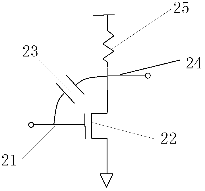
[0020] Please refer to Figure 4A , a substrate 41 is provided, a gate structure 42 is formed on the substrate 41, the substrate 41 includes a source region and a drain region, and the source region refers to the subsequent formation of a source extension region and a source re-doping The region of the impurity region, similarly, the drain region refers to the region where the drain extension region and the drain heavily doped region are to be formed later;

[0021] Please refer to Figure 4B , using the gate structure 42 as a mask...


PUM


Abstract

The invention provides a manufacture method of a metal oxide semiconductor (MOS) device for improving the frequency characteristics of a common source operation amplifier. Ion injection is carried out on the side wall layer by using neutral ions, the ion injection direction forms an included angle with the direction vertical to a substrate and is inclined towards the source electrode direction, and side walls with different morphologies are formed at the source terminal and the drain terminal of the MOS device of the common source operation amplifier, so after etching, the width of the side wall of a drain electrode is increased, and the width of the side wall of a source electrode is reduced, after the subsequent source drain doping injection and annealing process, the distance from the doping ions of the drain electrode to a device channel is increased, the distance from the doping ions of the source electrode to the channel is shortened, and the parasitic overlapping capacitance of the drain electrode is reduced under the condition of maintaining the device performance unchanged, so the frequency response characteristics of the common source operation amplifier are improved.

Description

technical field [0001] The invention relates to the field of semiconductor manufacturing, in particular to a method for manufacturing a MOS device for improving the frequency characteristic of a common source operational amplifier. Background technique [0002] CMOS (Complementary Metal Oxide Semiconductor) operational amplifier is one of the basic units of various circuits. With the development of information technology, the requirements for the processing speed of information data are higher and higher, and the requirements for the frequency response characteristics of the CMOS operational amplifiers used in them are also higher and higher. However, the parasitic capacitance of CMOS devices plays an increasingly negative role as the operating frequency increases. How to reduce the influence of these parasitic capacitances on CMOS operational amplifiers has become the key to improving the frequency response characteristics of CMOS operational amplifiers. [0003] Miller ca...

Claims


Application Information

Patent Timeline
Patent Type & Authority Applications(China)
IPC IPC(8): H01L21/336H01L21/3105H01L21/311
CPCH01L29/66659
Inventor 俞柳江
Owner SHANGHAI HUALI MICROELECTRONICS CORP
Why Eureka
Try Eureka