Method for improving frequency characteristic of common-source operational amplifier

A source terminal and gate technology, which is applied in the direction of improving amplifiers to improve efficiency, differential amplifiers, DC coupled DC amplifiers, etc., can solve the problems of reducing the frequency response characteristics of common source operational amplifiers, so as to improve frequency response characteristics and reduce Effect of Small Parasitic Overlap Capacitance

Inactive Publication Date: 2012-04-18
SHANGHAI HUALI MICROELECTRONICS CORP
View PDF3 Cites 1 Cited by
  • Summary
  • Abstract
  • Description
  • Claims
  • Application Information

AI Technical Summary

Problems solved by technology

There is a parasitic overlapping capacitance C between the output terminal and the input terminal of the common-source operational amplifier, that is, between the gate terminal and the drain terminal of the NMOS device 2 gd , which forms a feedback capacitor, therefore, due to the Miller effect, the parasitic overlap capacitance C gd will seriously degrade the frequency response characteristics of this common-source op amp

Method used


Image

  • Method for improving frequency characteristic of common-source operational amplifier
  • Method for improving frequency characteristic of common-source operational amplifier
  • Method for improving frequency characteristic of common-source operational amplifier

Examples


Embodiment Construction

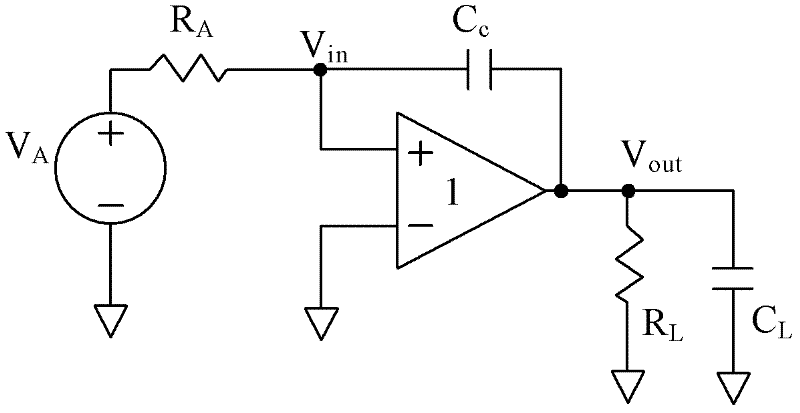
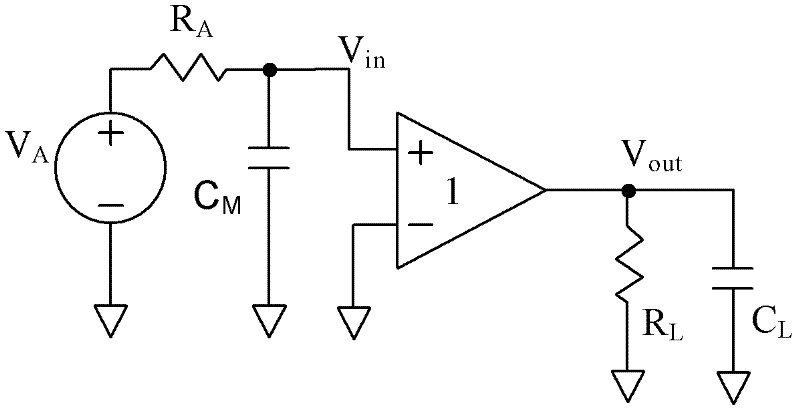
[0027] The following will combine Figure 3A-Figure 4C The above-mentioned spirit and essence of the present invention are described in detail.

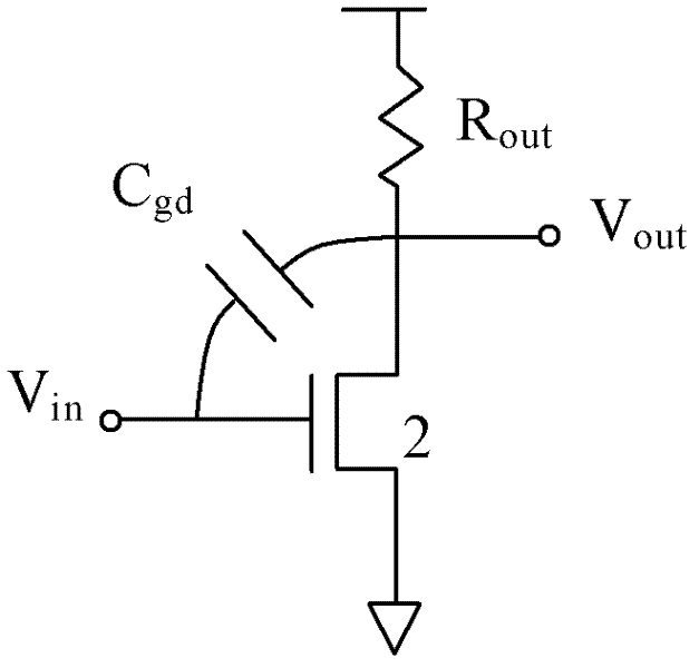
[0028] Figures 3A-3C Three steps in the process of fabricating an NMOS device in a common-source operational amplifier in the prior art are exemplarily shown.

[0029] Figure 3A A cross-sectional view of an NMOS device after sidewall deposition in the prior art is exemplarily shown. Such as Figure 3A As shown in , in the manufacturing process of NMOS devices in the prior art, in the first step, LDD (Lightly Doped Drain) structures 11 and 12, STI (Shallow Trench Isolation) structure 13 are first formed under the upper surface of the substrate 10 and 14 , and a gate 15 is formed above the upper surface of the substrate 10 . The LDD structures 11 and 12 are located on both sides below the gate 15 respectively, and are used to form a source terminal and a drain terminal and form an NMOS device together with the gate 15 . The STI...


PUM


Abstract

The invention provides a method for improving the frequency characteristic of a common-source operational amplifier. The method comprises the following steps of: etching at the first time, namely performing high transverse etching and low longitudinal etching on a spacer thin film above a first laser detector diode (LDD) structure for forming a source end and a spacer thin film which is positioned above a grid and arranged close to the first LDD structure; etching at the second time, simultaneously performing low transverse etching and high longitudinal etching on the spacer thin films corresponding to the upper sides of the source end, a drain end and the grid, so that a grid spacer corresponding to the upper side of the drain end is thickened and the grid spacer corresponding to the upper side of the source end is thinned; and high-doping and annealing exposed parts of the first LDD structure and a second LDD structure for forming the drain end respectively so as to form high-doped ion regions corresponding to the drain end and the source end respectively. The invention also provides a semiconductor device manufactured by using the method. The frequency response characteristic is improved.

Description

technical field [0001] The present application relates to the manufacture of semiconductor devices, more precisely, the present invention relates to a semiconductor device spacer etching method and semiconductor devices manufactured using the method. Background technique [0002] Complementary metal-oxide-semiconductor (CMOS) operational amplifiers are one of the building blocks of various circuits. With the development of information technology, the requirements for the processing speed of information data are getting higher and higher, and the requirements for the frequency response characteristics of the CMOS operational amplifiers used in it are also getting higher and higher. [0003] However, the parasitic capacitance of CMOS devices will produce more and more negative effects as the operating frequency increases. Therefore, how to reduce the influence of parasitic capacitance on CMOS operational amplifiers has become the key to improving the frequency response charact...

Claims


Application Information

Patent Timeline
IPC IPC(8): H03F3/45H03F1/02
Inventor 俞柳江
Owner SHANGHAI HUALI MICROELECTRONICS CORP
Why Eureka
Try Eureka