Detection method of metal nanometer film thickness

A metal nanometer and detection method technology, applied in the field of nanomaterials, can solve problems that affect the application, do not conform to the linear law, and the rate changes.

Inactive Publication Date: 2012-08-01
CHANGCHUN INST OF APPLIED CHEMISTRY - CHINESE ACAD OF SCI
View PDF4 Cites 11 Cited by
  • Summary
  • Abstract
  • Description
  • Claims
  • Application Information

AI Technical Summary

Problems solved by technology

The thickness of the nano-film has a great influence on its surface morphology and its conductivity, which in turn will affect its application
A variety of methods for detecting the thickness of metal nano-films are disclosed in the prior art. For example, according to the empirical rule that the thickness of the coating film increases linearly with the coating time, the thickness of the metal nano-film is calculated according to the coating time. Since the conditions of each coating film cannot Exactly the same, cause the rate of coating film to change, thereby do not conform to its linear law, make the detection result that this method obtains unreliable; The film thickness sensor method, howev

Method used


Image

  • Detection method of metal nanometer film thickness
  • Detection method of metal nanometer film thickness
  • Detection method of metal nanometer film thickness

Examples


Embodiment 1

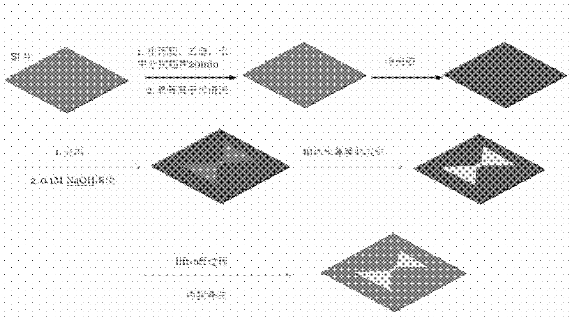
[0062] according to figure 1 The process flow shown prepares platinum nano-films with different thicknesses.

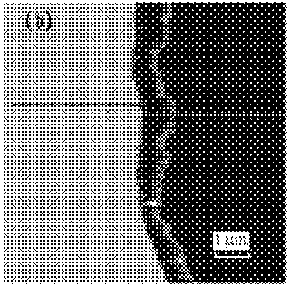
[0063] The obtained platinum nano-film is detected by an atomic force microscope in tapping mode, and the thickness of the platinum nano-film is obtained according to the obtained height map of the atomic force microscope.

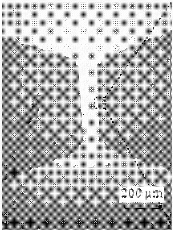
[0064] The result is as figure 2 and image 3 as shown, figure 2 For the optical micrograph of the platinum nanofilm prepared in Example 1 of the present invention, image 3 For the edge AFM height map of the platinum nanofilm prepared in Example 1 of the present invention, from image 3 The thickness of the platinum nanofilm can be obtained.

[0065] After obtaining the platinum nano-film, the present invention adopts the model to be the Hongda multimeter of DT 9204 to detect the resistance value of the platinum nano-film, according to the classical resistance law, obtain the relationship between the resistance value of the platinum nano-f...

Embodiment 2

[0068] The present invention selects the platinum nano-film prepared in embodiment 1, adopts the Hongda digital multimeter of DT 9204 to detect that the resistance value of the platinum nano-film is 29650 ohms, and calculates the platinum nano-film according to the standard curve obtained in embodiment 1. The thickness of nano film is 3.3nm; In order to verify the accuracy of method provided by the present invention, the present invention adopts atomic force probe microscope to detect the thickness of described platinum nano film with tapping mode, and the result is 3.2nm, the result is as shown in Table 1 Shown, table 1 is the detection result that embodiment 2~7 of the present invention obtains.

Embodiment 3

[0070] The present invention selects the platinum nano-film prepared in Example 1, adopts the Hongda digital multimeter of DT 9204 to detect and obtain the resistance value of the platinum nano-film to be 5520 ohms, and calculates the platinum nano-film according to the standard curve obtained in Example 1. The thickness of the nano film is 4.5nm; In order to verify the accuracy of the method provided by the present invention, the present invention uses an atomic force probe microscope to detect the thickness of the platinum nano film in a tapping mode, and the result is 4.6 nm, as shown in Table 1 Shown, table 1 is the detection result that embodiment 2~7 of the present invention obtains.


PUM

PropertyMeasurementUnit
Thicknessaaaaaaaaaa
Thicknessaaaaaaaaaa
Thicknessaaaaaaaaaa

Abstract

The invention provides a detection method of metal nanometer film thickness. The detection method includes detecting resistance value of the metal nanometer film to be detected; and according to the resistance value and a pre-established standard curve of the thickness of the metal nanometer film and the resistance value of the metal nanometer film, obtaining the thickness of the metal nanometer film through calculating, wherein the standard curve is a curve between logarithms of the resistance value of the metal nanometer film and reciprocals of the metal nanometer film thickness. According to the detection method, a good linearity exists between the resistance value of the metal nanometer film and the reciprocals of the metal nanometer film thickness, so that the standard curve between the metal nanometer film thickness and the resistance value is obtained; the thickness of the metal nanometer film can be obtained according to the standard curve and the resistance value of the metal nanometer film; and no complex operation process is required for detecting the metal nanometer film thickness, the detection method is simple and convenient, the detection speed is high, and the cost is low.

Description

technical field [0001] The invention relates to the technical field of nanometer materials, in particular to a method for detecting the thickness of a metal nanometer film. Background technique [0002] In the 21st century, due to the rapid development of information, biotechnology, energy, environment, national defense and other industries, newer and higher requirements are put forward for material performance, miniaturization, intelligence, high integration, high-density storage and ultra-fast transmission of components, etc. The size of materials is required to be smaller and smaller, and aerospace, new military equipment and trap manufacturing technology make the performance of materials extreme. Therefore, the research and innovation of new materials must be an important topic and development basis for future scientific research. Due to the special physical and chemical properties of nanomaterials, as well as the resulting special application value, it has become a hot ...

Claims


Application Information

Patent Timeline
IPC IPC(8): G01B7/06
Inventor 李壮温志伟张悦许富刚孙玉静石岩戴海潮
Owner CHANGCHUN INST OF APPLIED CHEMISTRY - CHINESE ACAD OF SCI
Why Eureka
Try Eureka