Transistor capable of improving tunnel penetration field effect

A field-effect transistor and tunneling technology, which is applied in the field of formation of enhanced tunnel penetration field-effect transistors, can solve the problems of not being able to suppress the bipolar conduction effect of the device well, the performance of the TFET device needs to be improved, and the operating speed of the device is reduced. Achieve the effects of suppressing the bipolar conduction effect, increasing the probability of tunnel penetration, and reducing the reverse control

Active Publication Date: 2014-11-26
TSINGHUA UNIV
View PDF4 Cites 0 Cited by
  • Summary
  • Abstract
  • Description
  • Claims
  • Application Information

AI Technical Summary

Problems solved by technology

As the size of tunneling field-effect transistors is getting smaller and smaller, especially for materials with narrow energy bands, such as Ge, InAs, InSb and other materials, the traditional structure cannot well suppress the bipolar conduction effect (Ambipolar Effect) of the device. ), leading to a sharp rise in the off-state current; at the same time, with the reduction of the feature size, the capacitance of the device, especially the gate-to-drain capacitance Cgd, takes a larger proportion, which makes the operating speed of the device decrease
The shortcoming of current prior art is that the performance of TFET device still needs to be improved

Method used


Image

  • Transistor capable of improving tunnel penetration field effect
  • Transistor capable of improving tunnel penetration field effect
  • Transistor capable of improving tunnel penetration field effect

Examples


Embodiment Construction

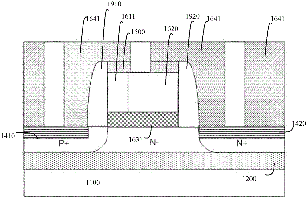
[0016] Such as figure 1 Shown is a diagram of an n-type enhanced tunneling field effect transistor according to an embodiment of the present invention. In the embodiment of the present invention, the n-type enhanced tunneling field effect transistor includes: a substrate 1100, a semi-insulating layer or insulating layer 1200, a channel region formed in the substrate 1100, and a channel region formed in the channel A source region and a drain region on both sides of the channel region, wherein the doping types of the drain region and the source region are opposite. The n-type enhanced tunneling field effect transistor further includes ohmic contact layers 1410 and 1420 on the source region and the drain region, and a gate stack formed on the channel region, wherein the gate stack includes a gate dielectric layer 1631, the gate stack further includes at least a first gate electrode 1611 and a second gate electrode 1620 distributed along the direction from the source region to t...


PUM


Abstract

A transistor capable of improving tunnel penetration field effect comprises a substrate, a channel region, a source region and a drain region, wherein the source region and the drain region are arranged on two sides of the channel region, and mixing types of the drain region and the source region are opposite. The transistor further comprises an ohmic contact layer and a gate stack. The gate stack comprises a gate dielectric layer, a first gate electrode, a second gate electrode, a first vacuum lateral wall and a second vacuum lateral wall, wherein the first gate electrode and the second gate electrode are arranged on the gate dielectric layer and have different work functions. The transistor increases carrier tunnel penetration probability from the source region to the channel region, and a certain distance is arranged between the gate stack and the drain region of a device so as to increase a bipolar window. Vacuum or an air lateral wall from a gate to the source region reduces inversion control of the gate on the source region. A transverse abnormal gate work function structure is led in the tunnel penetration field effect transistor, energy band distribution of the channel region is modulated, subthreshold slope of the transistor is remarkably reduced, driving current is increased, and performance of transistor devices is improved.

Description

technical field [0001] The invention relates to the technical field of semiconductor device design and manufacture, in particular to a method for forming an enhanced tunnel penetration field effect transistor. Background technique [0002] As the feature size continues to scale down, the size of traditional silicon field effect transistors gradually reaches the dual limits of physics and technology. Integrated circuits face many small size effects caused by materials and basic principles of devices, resulting in deterioration of device performance. For this reason, Improvement measures have been put forward, among which the tunneling field effect transistor (Tunneling Field Effect Transistor, TFET) is particularly prominent. As the size of tunneling field-effect transistors is getting smaller and smaller, especially for materials with narrow energy bands, such as Ge, InAs, InSb and other materials, the traditional structure cannot well suppress the bipolar conduction effect ...

Claims


Application Information

Patent Timeline
Patent Type & Authority Patents(China)
IPC IPC(8): H01L21/336
Inventor 梁仁荣刘立滨王敬许军
Owner TSINGHUA UNIV
Why Eureka
Try Eureka