Circuit board manufacturing process

A circuit board manufacturing and circuit board technology, applied in the direction of printed circuit manufacturing, printed circuit, printed circuit secondary processing, etc., can solve the problems of increasing the cost of gold plating on printed circuit boards, wasting gold salt materials, etc., to reduce the cost of gold plating, reduce effect of dosage

Inactive Publication Date: 2012-08-01
TAIWAN OASIS TECH CO LTD
View PDF4 Cites 4 Cited by
  • Summary
  • Abstract
  • Description
  • Claims
  • Application Information

AI Technical Summary

Problems solved by technology

[0005] However, in the manufacturing process of conventional printed circuit boards, the gold plating step is often arranged between the first copper and the second copper, and the copper foil substrate is fully gold-plated, and then the gold-plated layer at the electrode connection is etched with chemicals, not only A large amount of gold salt material is wasted, which relatively increases the gold plating cost of printed circuit boards

Method used


Image

  • Circuit board manufacturing process
  • Circuit board manufacturing process
  • Circuit board manufacturing process

Examples


Embodiment Construction

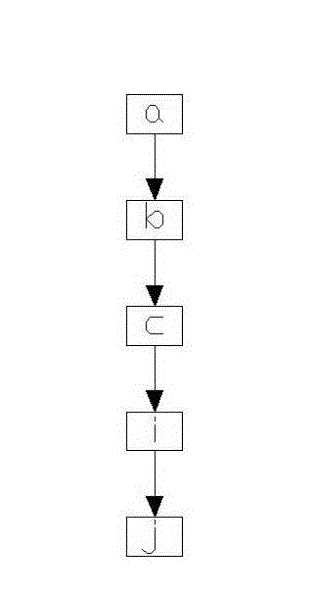
[0026] The circuit board manufacturing process of the present invention can be used to manufacture single-layer circuit board or multi-layer circuit board, take single-layer circuit board as example, as figure 1 As shown in the circuit board manufacturing flow chart of a preferred embodiment of manufacturing a single-layer circuit board according to the present invention, the circuit board manufacturing process of the present invention mainly includes the following steps.

[0027] a. Provide copper foil substrate; the copper foil substrate can be pre-cut to the size suitable for the factory process.

[0028] b. Duplicate a predetermined single-layer circuit pattern on the copper foil substrate; copy the drawn circuit pattern on the copper foil substrate by direct photoresist or indirect printing.

[0029] c. Remove the copper foil other than the circuit pattern of the copper foil substrate, so that a single-layer circuit layer composed of copper foil is formed on the copper fo...


PUM


Abstract

The invention discloses a circuit board manufacturing process and mainly provides the circuit board manufacturing process which can greatly reduce gold-plated cost. In the circuit board manufacturing process, a solder mask covers a non electrode joint of an outer copper foil substrate. Finally, gold-plated processing is performed on the outer copper foil substrate so that a gold-plated surface is established on the copper foil surface of the electrode joint which is not covered by the solder mask. Therefore, a gold-plated scope can be narrowed to the electrode joints, such as a bonding pad, a connecting line, an external electrode contact and the like. And a purpose of reducing the gold-plated cost can be achieved.

Description

technical field [0001] The invention relates to a circuit board manufacturing technology, in particular to a circuit board manufacturing process that can greatly reduce the cost of gold plating. Background technique [0002] Press, the printed circuit board [Printed circuit board (PCB)] will appear in almost every electronic device, in addition to fixing various electronic components, and providing electrical connections for each electronic component. At present, common printed circuit boards can be divided into single-sided boards, double-sided boards, multi-layer boards with four or more layers, and flexible boards. [0003] Generally speaking, the more complicated the functions of electronic products, the longer the loop distance, and the more contact pins, the more layers required for printed circuit boards, such as high-end consumer electronics, information and communication products, etc.; secondly, printed circuit boards In order to ensure the chemical resistance, ox...

Claims


Application Information

Patent Timeline
Patent Type & Authority Applications(China)
IPC IPC(8): H05K3/00H05K3/24
Inventor 李明顺林义顺
Owner TAIWAN OASIS TECH CO LTD
Why Eureka
Try Eureka