A low-cost packaging process for high-power electronic devices
A packaging process and technology for electronic devices, applied in electrical components, semiconductor/solid-state device manufacturing, circuits, etc., can solve the problem of high void rate of thermal interface soldering layer, troublesome solder paste coating process, and high price of gold-tin preformed solder. problems, to achieve the effect of reducing the void rate, reducing the process, and reducing the cost of gold plating
- Summary
- Abstract
- Description
- Claims
- Application Information
AI Technical Summary
Problems solved by technology
Method used
Image
Examples
Embodiment
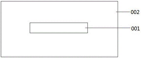
[0027] Such as figure 1 As shown, the chip 001 is pasted on the surface of the flange 002, using a gold-silicon eutectic soldering process or a gold-tin eutectic soldering process with a low void rate in the soldering layer.
[0028] Such as figure 2 As shown, a thick gold layer or gold-tin layer 005 is prepared on the back of the chip 001, the thickness of the thick gold layer or gold-tin layer 005 is between 1um-6um, the nickel-plated layer 003 on the surface of the flange 002, the nickel-plated layer 003 thickness is between Between 2um-15um, a thin gold layer 004 is plated on the nickel-plated layer 003, and the thickness of the thin gold layer 004 is between 25nm-1um. When the flange temperature exceeds the melting point of gold-silicon alloy or gold-tin alloy, a gold-silicon alloy or gold-tin alloy is formed between the chip 001 and flange 002, and they are firmly welded together to achieve gold-silicon eutectic welding or gold-tin eutectic welding Effect.
PUM
 Abstract
Description
Claims
Application Information

