Low-cost high-power electronic device packaging technology

A packaging process and technology for electronic devices, applied in electrical components, semiconductor/solid-state device manufacturing, circuits, etc., can solve the problem of high price of gold-tin preforms, troublesome solder paste coating process, and high void rate of thermal interface solder layers. problems, to achieve the effect of reducing the void rate, reducing the process, and reducing the cost of gold plating

Active Publication Date: 2014-10-01
长沙瑶华半导体科技有限公司
View PDF3 Cites 9 Cited by
  • Summary
  • Abstract
  • Description
  • Claims
  • Application Information

AI Technical Summary

Problems solved by technology

The price of gold-tin solder preforms is relatively high, and the process of applying solder paste is relatively troublesome, and the void rate of the thermal interface solder layer will be relatively high

Method used


Image

  • Low-cost high-power electronic device packaging technology
  • Low-cost high-power electronic device packaging technology

Examples


Embodiment

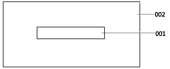
[0027] Such as figure 1 As shown, the chip 001 is pasted on the surface of the flange 002, using a gold-silicon eutectic soldering process or a gold-tin eutectic soldering process with a low void rate in the soldering layer.

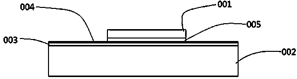
[0028] Such as figure 2 As shown, a thick gold layer or gold-tin layer 005 is prepared on the back of the chip 001, the thickness of the thick gold layer or gold-tin layer 005 is between 1um-6um, the nickel-plated layer 003 on the surface of the flange 002, the thickness of the nickel-plated layer 003 is Between 2um-15um, a thin gold layer 004 is plated on the nickel-plated layer 003, and the thickness of the thin gold layer 004 is between 25nm-1um. When the flange temperature exceeds the melting point of gold-silicon alloy or gold-tin alloy, a gold-silicon alloy or gold-tin alloy is formed between the chip 001 and flange 002, and they are firmly welded together to achieve gold-silicon eutectic welding or gold-tin eutectic welding Effect.


PUM


Abstract

The invention discloses a low-cost high-power electronic device packaging technology. The technology comprises the steps that a chip and flange for packaging a high-power electronic device are prepared, a thick gold layer or a gold-tin layer is manufactured on the back face of the chip, a nickel layer and a thin gold layer are plated on the surface of the flange in sequence, and the chip and the flange are in surface mounting through gold-silicon eutectic welding or gold-tin eutectic welding. According to the low-cost high-power electronic device packaging technology, the thick gold layer or the gold-tin layer is manufactured on the back face of the chip, and the thin gold layer is plated on the surface of the flange, so that the good effect of gold-silicon eutectic welding or gold-tin eutectic welding is achieved, the void content of a hot interface layer between the chip and the flange is reduced, the radiating efficiency of the chip is ensured, the gold plating cost in the packaging technology is greatly reduced, and the number of working procedures is reduced.

Description

technical field [0001] The invention relates to the field of packaging technology of high-power electronic devices, in particular to a low-cost packaging technology of high-power devices. Background technique [0002] High-power electronic devices have relatively high heat dissipation requirements. When the chip is attached to the flange, it is necessary to ensure that the void in the thermal interface layer between the chip and the flange is as small as possible. Gold-silicon eutectic soldering and gold-tin eutectic soldering are currently the best chip placement method. At present, gold-silicon eutectic soldering mainly uses a thick gold layer plated on the flange and the silicon of the chip itself to form a gold-silicon alloy at a eutectic temperature above 363°C to achieve a good patch effect. Gold-tin eutectic soldering mainly adopts the method of coating gold-tin solder paste or gold-tin preform to realize chip soldering. The gold-silicon eutectic welding process req...

Claims


Application Information

Patent Timeline
Patent Type & Authority Applications(China)
IPC IPC(8): H01L21/50H01L21/60
CPCH01L21/4882
Inventor 马文珍张耀辉曾大杰彭虎
Owner 长沙瑶华半导体科技有限公司
Why Eureka
Try Eureka