TFT array substrate, liquid crystal display panel method for manufacturing the array substrate

An array substrate and active layer technology, which is applied in semiconductor/solid-state device manufacturing, transistors, optics, etc., can solve the problems that affect the display effect of liquid crystal panels, and the spacers are easy to fall over, so as to improve the display effect and prevent the effect of falling over.

Inactive Publication Date: 2012-08-08
BEIJING BOE OPTOELECTRONCIS TECH CO LTD
View PDF3 Cites 7 Cited by
  • Summary
  • Abstract
  • Description
  • Claims
  • Application Information

AI Technical Summary

Problems solved by technology

[0004] After the spacer is placed, when the liquid crystal panel is squeezed by an external force, the spacer on the TFT array substrate is easy to fall, and after fall...

Method used


Image

  • TFT array substrate, liquid crystal display panel method for manufacturing the array substrate
  • TFT array substrate, liquid crystal display panel method for manufacturing the array substrate
  • TFT array substrate, liquid crystal display panel method for manufacturing the array substrate

Examples


Embodiment 1

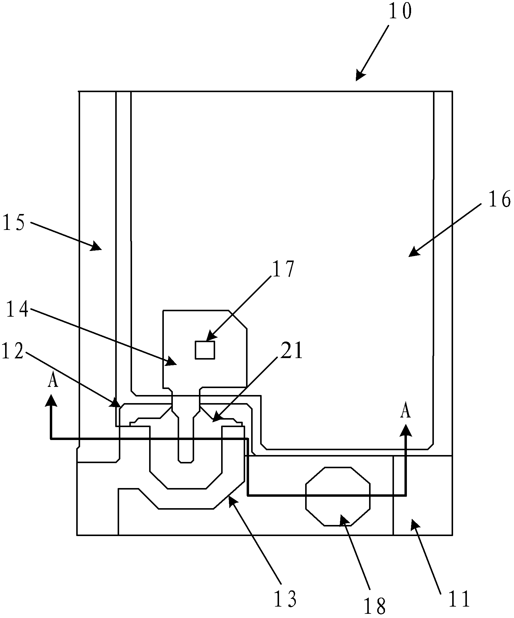
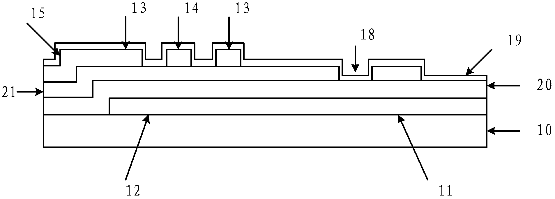
[0032] The TFT array substrate provided by the embodiment of the present invention, such as figure 1 , figure 2 as shown, figure 1 is a schematic top view of the structure of a pixel region of the TFT array substrate, figure 2 for figure 1 The shown cross-sectional view of the TFT array substrate along the direction A-A.

[0033] The TFT array substrate includes: a substrate 10; a gate line 11 and a gate 12 formed on the substrate 10; a gate insulating layer 20 formed on the gate line 11 and the gate 12; a semiconductor active layer formed on the gate insulating layer 20 Layer 21, formed on the source electrode 13, the drain electrode 14, and the data line 15 above the semiconductor active layer 21; there is a groove 18 on the semiconductor active layer 21 above the gate line 11; in addition, on the data line 15, the source electrode 13. A protection layer 19 is formed above the drain electrode 14; a pixel electrode 16 is formed in the area surrounded by the intersection...

Embodiment 2

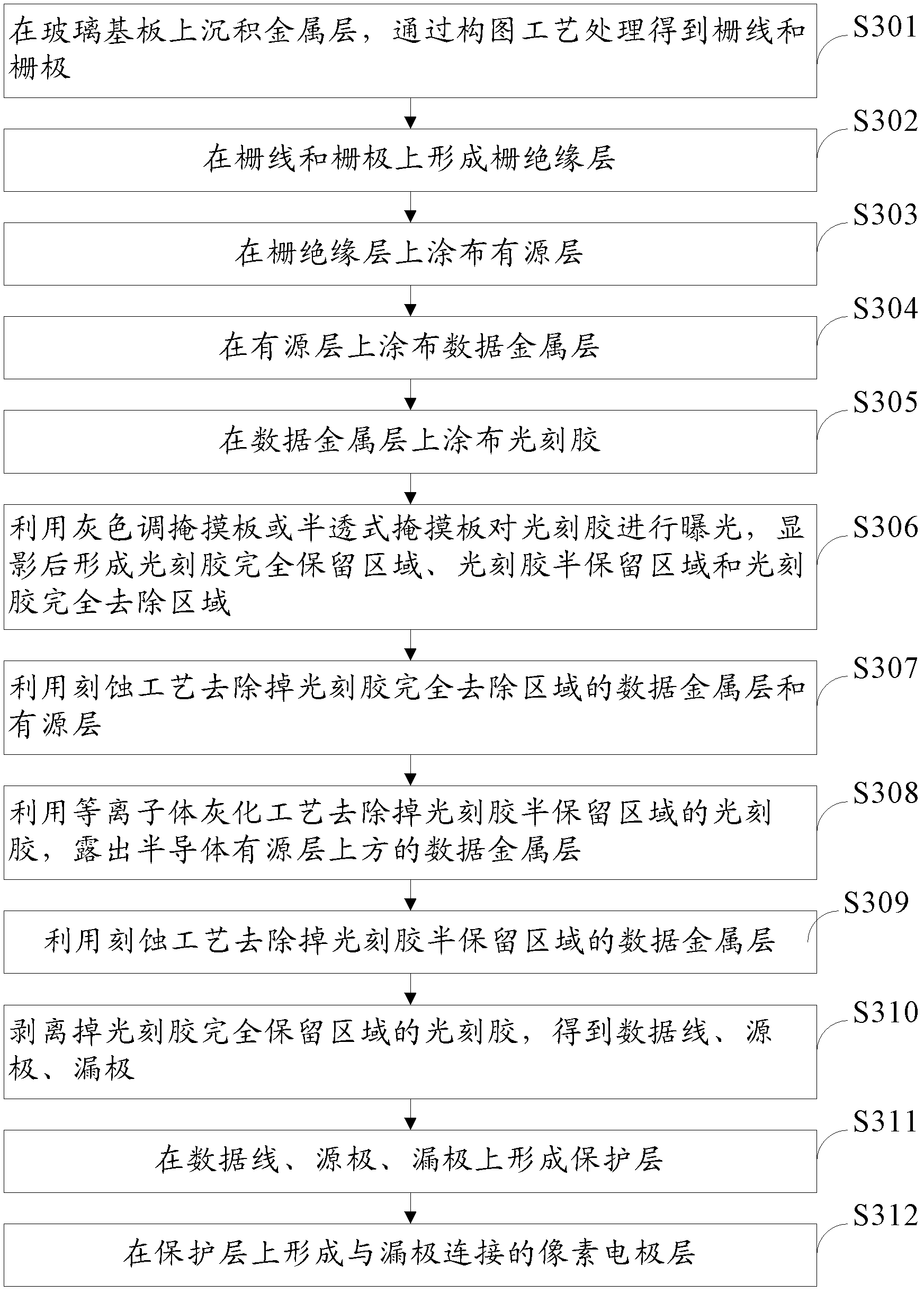
[0036] Attached below Figure 3 ~ Figure 13 As shown, the method for manufacturing the TFT array substrate provided by the embodiment of the present invention will be described. In this example Figure 4 ~ Figure 13 Both are with figure 2 same section position. Such as image 3 As shown, the method steps include:

[0037] S301 , depositing a metal layer on a glass substrate, and obtaining gate lines 11 and gates 12 through a patterning process.

[0038] Such as Figure 4 As shown, the magnetron sputtering method can be used to prepare a layer with a thickness of to metal film layer. The metal material can usually be metals such as molybdenum, aluminum, aluminum-nickel alloy, molybdenum-tungsten alloy, chromium, or copper, or a combination structure of the above-mentioned thin films. Then, a plurality of horizontal grid lines 11 and gates 12 connected to the grid lines are formed on a certain area of ​​the glass substrate 10 through a first patterning process such a...

Embodiment 3

[0057] The liquid crystal display panel provided by the embodiment of the present invention, such as Figure 14 As shown, it includes a composite TFT array substrate 80 and a color filter substrate 70, and the TFT array substrate 80 is the TFT array substrate provided in the second embodiment above, wherein the TFT array substrate 80 and the color filter substrate 70 The spacers 60 are located in the grooves 18 formed by the semiconductor active layer 41 of the TFT array substrate 80 .

[0058] In the liquid crystal display panel provided by the embodiment of the present invention, the spacer between the TFT array substrate and the color filter substrate is placed in the groove formed by the semiconductor active layer above the gate line, and when the liquid crystal panel is squeezed by external force, it can prevent The spacer falls and touches the alignment film, thereby improving the display effect of the liquid crystal panel.

[0059] In the liquid crystal display panel p...


PUM


Abstract

The invention, which relates to the liquid crystal display panel manufacturing field, discloses a thin film transistor (TFT) array substrate, a liquid crystal display panel method for manufacturing the array substrate, so that toppling of a space can be prevented and a display effect of a liquid crystal panel is improved. The method for manufacturing a TFT array substrate comprises the following steps that: an active layer is coated on a substrate provided with a gate line, a gate electrode and a gate insulating layer; a data metal layer is coated on the active layer and a data line, a source electrode, a drain electrode, a semiconductor active layer and a groove on the semiconductor active layer above the gate line are obtained by processing according to a composition process; a protective layer is formed on the data line, the source electrode and the drain electrode; and a pixel electrode layer connected with the drain electrode is formed on the protective layer. According to the invention, the TFT array substrate, the liquid crystal display panel the method for manufacturing the array substrate are applied to manufacturing of the liquid crystal display panel.

Description

technical field [0001] The invention relates to the field of manufacturing liquid crystal display panels, in particular to a TFT array substrate, a liquid crystal display panel and a method for manufacturing the array substrate. Background technique [0002] At present, the liquid crystal display panel of TFT-LCD (Thin Film Transistor-Liquid Crystal Display, Thin Film Field Effect Transistor Liquid Crystal Display) is composed of two upper and lower glass substrates formed in a box and a liquid crystal layer filled in the middle. [0003] In order to control the cell thickness, spacers are generally used for support, wherein the spacers are mainly placed in the non-light-transmitting regions of the TFT array substrate. [0004] After the spacer is placed, when the liquid crystal panel is squeezed by an external force, the spacer on the TFT array substrate is easy to fall, and after falling, it is easy to touch the alignment film on the TFT array substrate or be incorporated ...

Claims


Application Information

Patent Timeline
IPC IPC(8): H01L21/77H01L27/02H01L29/786G02F1/1362G02F1/1368G02F1/1339
Inventor 薛艳娜陈小川黎蔚王世君
Owner BEIJING BOE OPTOELECTRONCIS TECH CO LTD
Why Eureka
Try Eureka